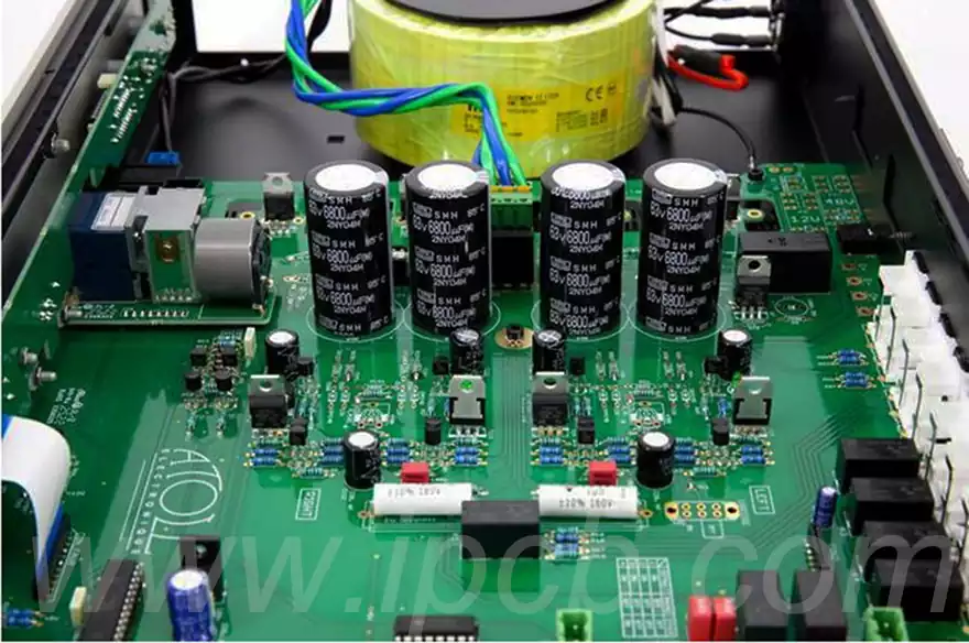
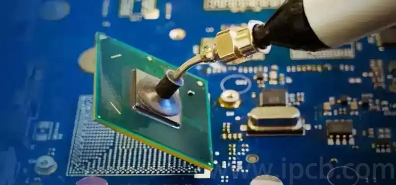
Through hole soldering is a method of fixing electronic components on a PCB (Printed Circuit Board). Through holes are drilled to form through holes in the PCB, then components are inserted into the through holes, and then the solder is melted between the PCB and the component terminals by heating to realize the soldering. Through hole soldering is widely used in the electronics industry, such as computer motherboards, mobile communication devices and other fields.
Through hole soldering technique is a soldering method in which long, thin leads are inserted into the round holes of a printed wiring board (PWB), and then solder is applied to stick the leads and the PWB copper foil.The through hole soldering technique is realized by the structure of 3 parts on top of the through-hole: drilling holes, copper foil and solder pads. It is mainly categorized into manual pin soldering, wave soldering, surge soldering, counter-current (wave) soldering and surface mount (SMT) methods.
Process Flow
- Drilling: First of all, it is necessary to make through-holes on the PCB by drilling holes to match the copper soldering disks of the electronic components.
- Manual or automatic insertion of components: the electronic components to be soldered are inserted into the PCB through the through-hole.
- Wave soldering: Put the PCB into the wave soldering equipment, then heat the soldering area to a certain temperature, in this process the solder will be melted and coated on the PCB to realize the soldering.
- Inspection: After completing the welding, check the quality of the solder joints through quality inspection. Check whether the solder joints are smooth and flat, and whether there is any soldering deficiency and un-soldered condition.
Through hole soldering method:
- Manual welding
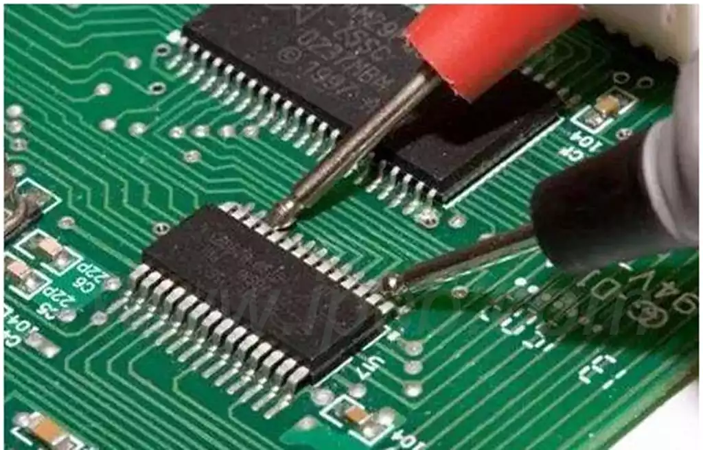
Suitable for very small batch sizes. The quality of the weld depends on the training,experience and skills received by the operator.The level of weld quality of the operator can be improved through training courses and standards.
Advantages: Inexpensive. Disadvantages: Labor intensive work, weld quality depends entirely on the skill level of the operator. - Dip welding
With this method of soldering, the staff needs to be close to the very hot solder pots and flux fumes in the air in contact with the link,so this method is more difficult to do, and the staff may also be dangerous.
Advantages: low soldering cost per joint,faster soldering speed.Disadvantages:obsolete technology, small production batch, the welding process is messy and dangerous, welding is not very precise,some short-circuiting between the solder joints,need to carry out some checks and rework. - Torch welding
At present, the use of butt welding is rare, the current market has been replaced by the common wave soldering.
Points: the cost is lower than the wave soldering,butt soldering system occupies less space. Disadvantages: Slow operation, may lead to short circuit, need to rework. - Wave soldering
Wave soldering is currently the most commonly used and most effective method, wave soldering system has a large enough solder pot to handle the maximum width of the board you expect.Wave soldering is suitable for medium or high volume soldering.
Pros: High return on investment, the entire soldering process is controllable and repeatable, and operators can be brought on board with simple training. Disadvantages: the cost of wave soldering system is higher than the previous mentioned several welding methods, but it is the lowest welding cost per circuit board, wave soldering system in the workshop occupies more space. - Selective soldering
Selective soldering is a special type of soldering.Selective soldering is the only good way to solder through hole components on circuit boards when the circuit tubes are already fitted with other components and through hole components can no longer be fitted using a wave soldering system.
Pros: good repeatability and environmental controllability, scalable, can increase throughput by adding modules. Disadvantages: quite expensive, slow, requires intensive operator training, training can be minimized with software options, each specific selective soldering process is related to the pcb layout.
Basic requirements for through hole soldering solder joints:
Good electrical conductivity:the solder joint must be able to conduct electricity efficiently to ensure the smooth transmission of current.
Welding strength:the solder joint must have sufficient mechanical strength to withstand mechanical and thermal stresses.
Thermal conductivity:the welded joint must have good thermal conductivity to disperse and transfer the heat generated during the welding process.
Corrosion resistance:the solder joint must have a certain degree of corrosion resistance to ensure that it can remain stable in harsh environments.
Appearance quality:Welded joints must be smooth and clean to ensure that their appearance is aesthetically pleasing and meets quality standards.
The through hole reflow soldering process is the use of reflow soldering technology to assemble through-hole and shaped components. The manufacturing process steps used to assemble printed circuit boards (PCBs) depend largely on the particular components used in the assembly.Due to the increasing emphasis on miniaturization, increased functionality, and higher component densities, many single- and double-sided boards are dominated by Surface Mount Components (SMCs). However, due to factors such as inherent strength, reliability, and fitness for purpose, through-hole devices are still preferred over SMCs in some cases, especially for connectors at the edge of the PCB board.
The disadvantage of using through-hole devices on boards with predominantly surface-mounted assemblies is the high cost of individual solder joints because of the additional processing steps involved,including wave soldering,hand soldering,or other selective soldering methods.The key to this type of assembly is the ability to provide simultaneous reflow for both through hole and surface mounted components in a single, integrated process.
The through-hole reflow (or THR) process enables simultaneous reflow of both through-hole and SMC devices in a single step.The steps required for the manufacturing process depend on the particular components used in the assembly.For example,a computer motherboard has a large number of SMCs,which make up the majority of the components used, and a limited number of through-hole devices: connectors,discrete assemblies,switches and jack devices, etc. Currently solder paste stencil printing and reflow soldering are used to secure the SMCs to the PCB substrate.A similar process can be used to accomplish the interconnection of through-hole as well as shaped devices.In many cases,the use of the THR process eliminates the need for subsequent wave soldering operations.
Advantages of the through hole reflow soldering process include:
- Existing SMT equipment can be utilized to assemble the THC/THD,resulting in cost and investment savings.
- Current automated multifunctional placement equipment can be used to place THC/THD.By using THR on PCBs that are primarily surface mounted,traditional wave soldering and manual insertion processes can be discarded,and a single SMT production line can be used to complete the assembly of all PCBs.
- Integrates multiple operations and simplifies the process.
- Requires less equipment,materials and personnel.
- It can reduce the production cost and shorten the production cycle.
- It can reduce the high defect rate brought by wave soldering.
- One or more heat treatment steps can be eliminated,thus improving solderability and reliability of electronic assemblies.
However,the through hole reflow soldering process also has some disadvantages: - The amount of solder paste used is large.
- Solder paste evaporation will form more residue,which may cause contamination of the machine and PCB.
- Solder joints may produce voids.
- Through-hole components need to withstand high temperature shock of 240℃ for 30 seconds,and need to meet specific thermal stability requirements.
- The standard for through-hole solder joints requires that the solder wetting angle exists and that the solder fills at least 100% of the circuit board thickness of the through-hole,which poses a technical challenge toTHR.Since the volume of the metal component in the solder paste accounts for about half of the total volume, it is necessary to optimize the design of the through-hole pads and stencils to ensure that the amount of solder paste is sufficient to avoid tin defects and cavities.
- Compared with the traditional wave soldering process,THR is technically more difficult.The shape of the solder joints will be affected by factors such as PCB thickness,plated hole size,pad size,solder paste printing volume,component lead diameters,and pin spacing.In addition,the amount of filler metallization hole solder is also related to the opening size of the printed stencil.
With many advantages such as high quality, low cost, long life and high productivity,through hole soldering technology is widely used in electronic assembly and PCB manufacturing.In the automated production process,through-hole soldering technology can realize high-speed parallel,high-precision and high-reliability electronic assembly.Specific applications include automotive electronics, aerospace,medical devices,smartphones and computers.
Through hole soldering technology occupies an important position in electronics manufacturing due to its robustness and flexibility.The revolutionary application of through hole reflow soldering is promoting the double improvement of production efficiency and product quality,heralding a more efficient and intelligent future for the electronics manufacturing industry.