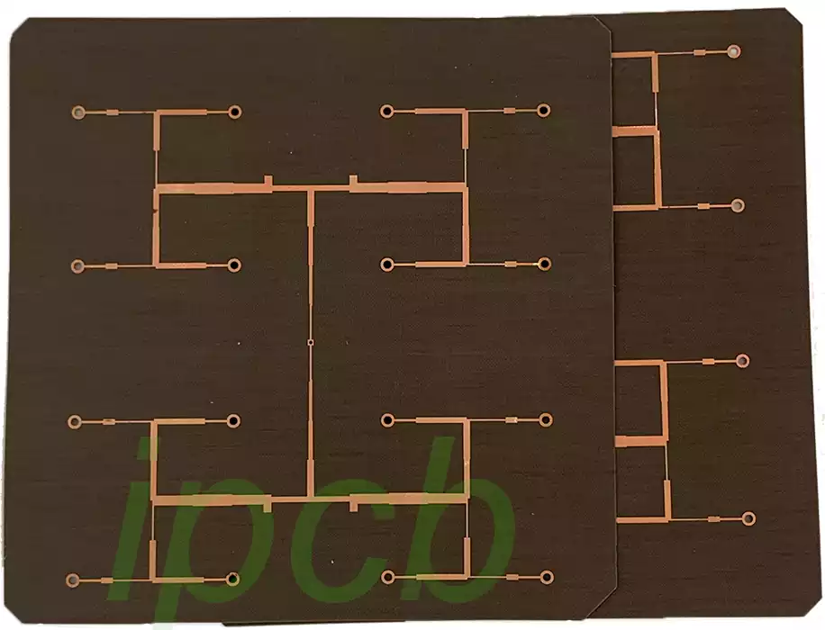
Ceramic multilayer PCB board refers to the multilayer circuit boards used in electrical products, multilayer boards with more single-sided or double-sided wiring board. With a double-sided for the inner layer, two single-sided for the outer layer or two double-sided for the inner layer, two single-sided for the outer layer of the printed circuit board, through the positioning system and insulating bonding material alternating with the conductive graphics according to the design requirements for interconnecting printed circuit boards have become four-layer, six-layer printed circuit boards, also known as multilayer printed circuit boards.
With the continuous development of SMT (surface mount technology), as well as a new generation of SMD (surface mounted devices) continue to launch, such as QFP, QFN, CSP, BGA (especially MBGA), so that the electronic products are more intelligent, miniaturization, and thus promote a major reform of the PCB industry technology and progress. Since 1991, IBM first successfully developed a high-density multilayer board (SLC) since the countries of the major groups have developed a variety of high-density interconnect (HDI) microvia board. The rapid development of these processing technologies, prompting the design of the PCB has been gradually to multi-layer, high-density wiring direction. Multilayer PCB board with its flexible design, stable and reliable electrical performance and superior economic performance, is now widely used in the manufacture of electronic products.
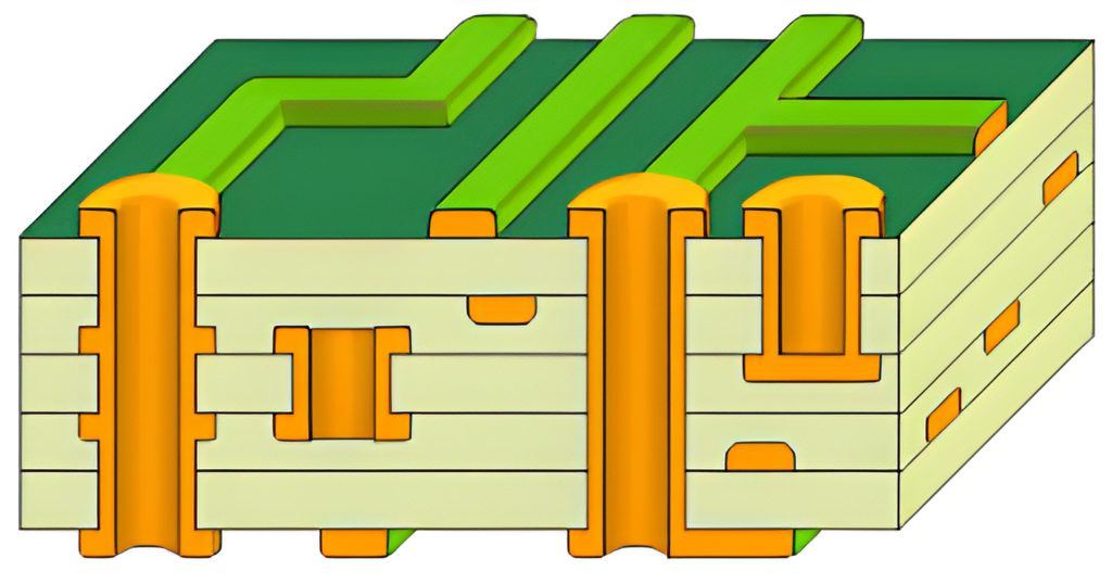
ceramic multilayer pcb with single-sided and double-sided board between the biggest difference is the increase in the internal power supply layer and ground layer. Power and ground networks are routed primarily on the power layer. Each substrate layer on a multilayer PCB board has conductive metal on both sides and special adhesives are used to join the boards together and eye the presence of insulation between each board. However, PCB multilayer wiring is primarily based on the top and bottom layers, supplemented by intermediate wiring layers. Therefore, the design of multilayer PCB boards is essentially the same as that of double-sided boards. The key is how to optimize the wiring of the internal electrical layers in order to make the circuit board wiring more reasonable. The inevitable product of multifunctional development, large capacity and small size.
PCB is a circuit board manufactured in a similar way to printing, so common PCBs are several layers bonded together, each with a resin insulating substrate and a metal circuit layer. The most basic PCB is divided into four layers, the top and bottom layers of circuitry are functional circuits, arranging the most important circuits and components, while the middle two layers of circuitry are the ground and power layers. The advantage of this is to be able to make corrections to the signal lines, but also better shielding against interference. Generally speaking, 4 layers can already meet the normal operation of the PCB, then the so-called 6 layers, 8 layers, 10 layers, in fact, is to add more layers of circuitry to enhance the electrical capacity of the PCB, that is, the pressure capacity. Therefore, the increase in the number of PCB layers means that more circuits can be designed inside.
What are the qualities of ceramic multilayer PCBs?
Ceramic multilayer PCBs have several special attributes that make them superior to other ceramic board types.
These attributes include:
Ceramic multilayer PCBs offer typical thermal conduction with a reduced coefficient of thermal expansion.
As a result, they provide reliable performance for high power circuits. Given its simplicity of design and higher level of performance, ceramic multilayer PCB is a very nice find. Therefore, it can replace the time-honored ceramic circuit boards.
In addition, you find that ceramic multilayer PCBs can operate properly at elevated temperatures in excess of 300°C. The boards can therefore withstand external temperatures. As a result, the board can withstand external temperature fluctuations without affecting the board’s performance. By manufacturing multilayer ceramic circuit boards, you will find that they can be made smaller and still be functionally reliable. With small board systems, devices can be made even smaller, allowing for high mobility and portability. The frequency performance achieved by ceramic multilayer PCBs is admirable. In such a setup, signal interference during transmission is reduced due to dedicated signal planes. Manufacturing multilayer ceramic PCBs is often more cost-effective than manufacturing single-layer boards with the same number of layers. With multilayer PCB design, you can have a denser stack of bundled layers. You also find that you can encapsulate multilayer ceramic PCBs in a sealed enclosure that prevents moisture and water penetration. This prevents damage to the board’s dielectric properties.
Ceramic multilayer PCB has the following advantages:
- High Thermal Conductivity: Ceramic materials inherently have high thermal conductivity for efficient heat dissipation. This characteristic is especially useful in high power or high temperature applications where managing thermal loads is critical.
- Low Coefficient of Thermal Expansion (CTE): Ceramics have a low coefficient of thermal expansion, meaning they expand less when heated. This is critical in electronics, where varying expansion rates between materials can lead to mechanical stress and potential failures.
- Excellent electrical insulation: Ceramic multilayer PCBs have excellent electrical insulation. Their ability to withstand high voltages and provide excellent isolation between electrical components is critical to the reliability and safety of electronic circuits.
- Chemical Resistance: They are chemically stable and can withstand exposure to corrosive chemicals without degradation. This makes them suitable for use in chemically harsh environments.
- High Mechanical Strength: Ceramic materials are known for their high mechanical strength and stiffness, providing a sturdy platform for mounting heavy or sensitive components.
- High Frequency Performance: Ceramic multilayer PCBs exhibit excellent high frequency performance due to their low dielectric constant and loss angle tangent. This makes them an excellent choice for RF (radio frequency) and microwave applications.
- Long-term stability: They exhibit long-term stability under varying environmental conditions, making them reliable for use in a variety of applications over the long term.
- Hermeticity: Ceramic multilayer PCBs can be hermetically sealed, which is useful for applications that require an airtight enclosure to protect sensitive electronic equipment from environmental contaminants.
- Fine Line Handling: The material properties of ceramics allow for fine line circuits and higher resolution in circuit design, which is very beneficial in miniaturization and high density circuit applications.
Disadvantages:
Increased cost: Compared to single-layer boards, ceramic multilayer PCBs are more complex to manufacture and require more sophisticated equipment and techniques, thus increasing the cost accordingly.
Difficulty in design: Multilayer design involves more wiring rules and signal integrity considerations, which requires higher professional skills for designers, and the design cycle may be longer.
Difficulty in maintenance: Once a multilayer board fails, due to its complex internal structure, it is relatively difficult to locate and repair the problem, and sometimes even need to be completely replaced.
Long production cycle: The production process of ceramic multilayer PCB includes multiple steps such as lamination, drilling, copper plating, etc. Compared with single-layer boards, the overall production cycle is longer.

What are the uses of ceramic multilayer PCBs?
Considering the increased circuit and board space that multilayer PCBs add, you will find multiple uses for multilayer PCBs.
Ceramic multilayer PCBs are used for memory modules. These modules can be produced by connecting integrated circuit chips in a four-layer setup.
The multilayer ceramic PCBs used in these devices offer higher density and impressive performance.
You would expect multilayer ceramic PCBs to be used in aerospace developments such as satellite telecommunications and space mobility devices.This complements military weapons such as missiles. In these applications, multilayer ceramic PCBs are favored for their excellent performance in harsh environments. You’ll find that multilayer PCBs have impressive resistance to applied shock, heat, and vibration.
Ceramic multilayer PCBs are used in miniaturized devices such as electronic equipment. They are useful because the multilayer configuration allows for the connection of a greater number of electronic components. This realization appropriately improves gadget performance.
Another modular application for ceramic multilayer PCBs is in transceiver modules. In this regard, you will find multilayer ceramic PCBs specialized for radio detection and ranging communications. The module is used for the transmission and reception of radio frequency signals. In this case, the ceramic substrate is made of aluminum nitride because it has a higher thermal conductivity than alumina. In addition, it has a low CTE, which provides an ideal transmission path for interference-free communications.
Some common applications for ceramic multilayer PCBs include:
- High Power Electronics: Ceramic PCBs are ideal for high power electronics because of their excellent thermal conductivity, which contributes to efficient heat dissipation. This is critical to ensuring the reliability and extended life of power electronics such as power converters, inverters and amplifiers.
- LED Lighting: The high thermal conductivity of ceramic PCBs is very beneficial in LED applications as it helps to effectively manage the heat generated by LEDs. This is critical to maintaining the performance and longevity of LED lamps, especially in high power LED lighting systems.
- Automotive electronics: Ceramic PCBs are used in the automotive industry, particularly in power modules, sensors and control units for electric and hybrid vehicles. With a low coefficient of thermal expansion (CTE), high thermal conductivity and mechanical strength, ceramic PCBs are well suited for harsh and demanding automotive environments.
- Aerospace and Defense Electronics: The aerospace and defense sectors require highly reliable electronics that can withstand harsh environments. Ceramic PCBs are resistant to high temperatures, vibration, and corrosive chemicals, making them ideal for applications such as radar systems, communications equipment, and avionics.
- Radio Frequency (RF) and Microwave Electronics: Ceramic PCBs are well suited for RF and microwave applications due to their low dielectric constant and loss angle tangent. They ensure better signal integrity and performance for high frequency electronics such as antennas, RF filters and microwave circuits.
- Medical Devices: In medical electronics, ceramic PCBs are used in imaging systems, patient monitoring devices and diagnostic equipment. Their ability to be sealed is critical to protecting sensitive electronics from contamination, moisture and other environmental factors.
- Industrial electronics: ceramic multilayer pcb are used in a variety of industrial electronics applications, including sensors, control systems and power modules. Their chemical resistance and mechanical strength make them suitable for harsh industrial environments.
- Telecommunications: The telecommunications industry benefits from the use of ceramic PCBs in applications such as base stations, satellite communications and signal amplification systems where high frequency performance and thermal management are critical.
- Consumer electronics: While ceramic PCBs are typically more expensive, they are used in high-end consumer electronics where performance, miniaturization and aesthetics are important, such as smartphones, wearables and high-definition displays.
Ceramic Multilayer PCB Manufacturer
Since 2012, iPCB has been providing ceramic PCB manufacturing services. Our ceramic PCB materials include Aluminum Oxide (Al2O3), Aluminum Nitride (AlN, ALN), Silicon Nitride (SiN), Beryllium Oxide (BeO), Boron Nitride (BN), Silicon Carbide (SiC) and Zirconium Oxide (ZrO2).
iPCB fabricates ceramic PCBs utilizing DCB, DAB, thick film, and active metal brazing (AMB) technologies. iPCB has a strong ceramic PCB fabrication capability to meet your requirements and better fulfill your PCB design requirements.