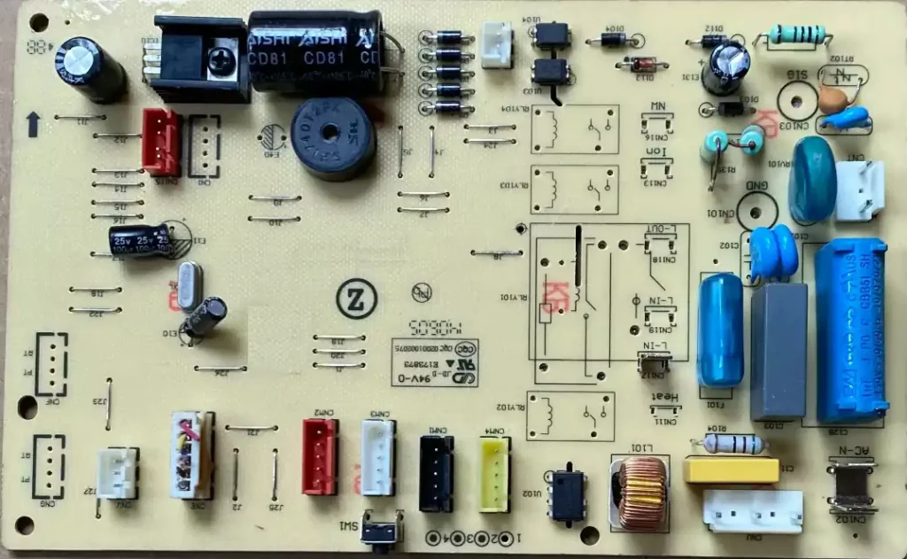
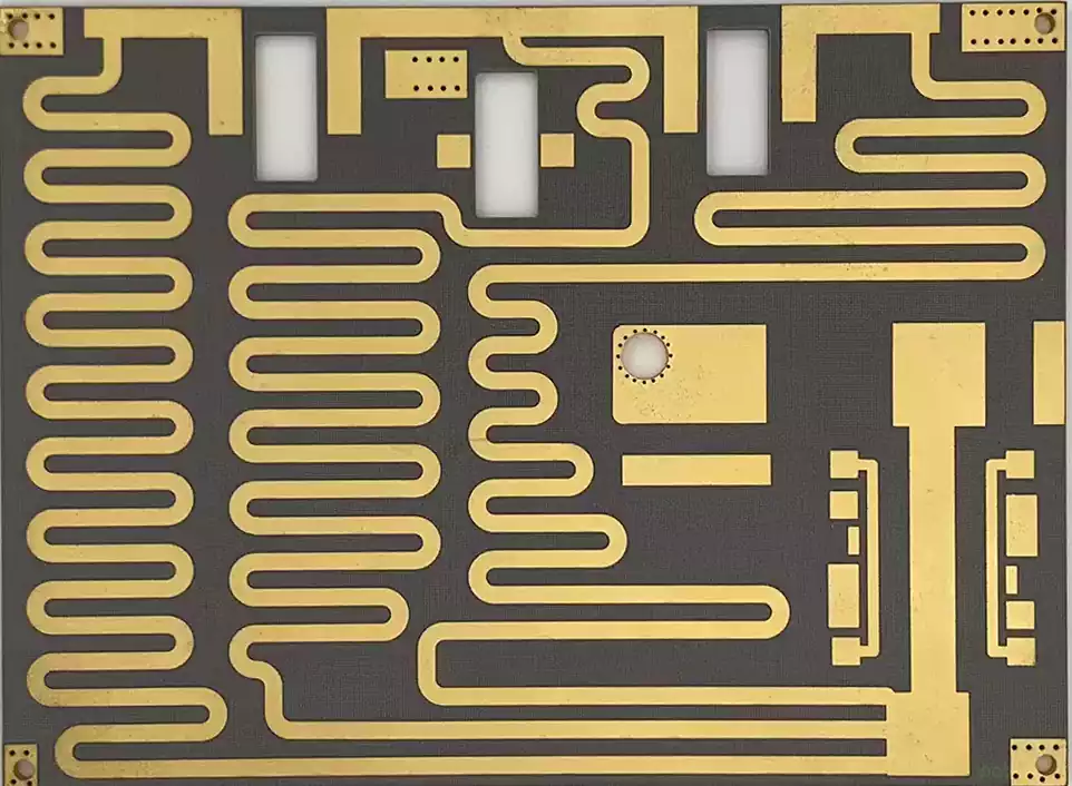
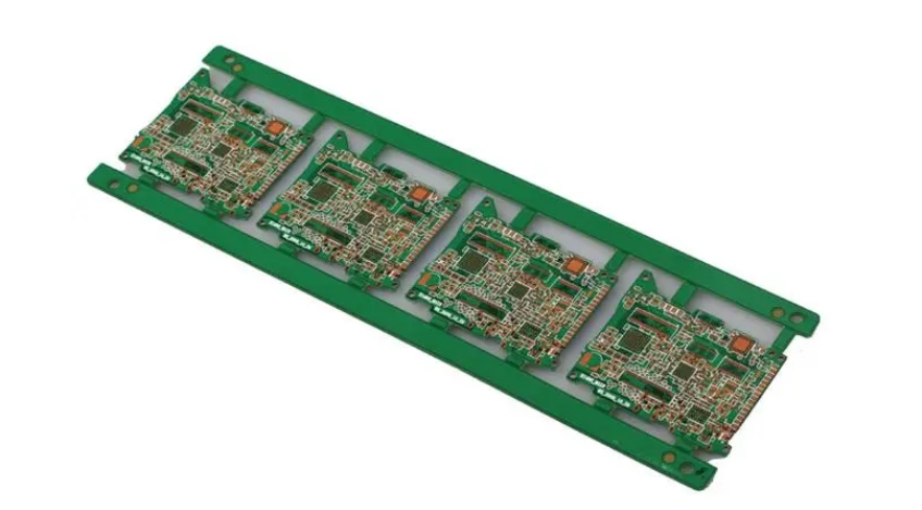
RF PCB stackup involves combining multiple board layers in a specific order and structure to form a complex circuit board. This structure not only accommodates the different functions of the circuits, but also ensures that interference between components is as low as possible and signal transmission is as stable as possible in the presence of high-frequency signals. This is especially important for devices that require high performance and high frequency operation.
Factors for material selection for RF PCB stackup:
Dielectric Constant (Dk)
Dielectric constant (Dk) is a key measure of a material’s ability to store electrical energy; the lower its value, the faster the signal propagation rate. In radio frequency (RF) applications,choosing the right dielectric constant is critical to the speed of signal transmission and electromagnetic compatibility of the circuit. Materials with low dielectric constants often significantly improve the performance of RF circuits because they reduce signal delay and distortion and improve overall signal integrity.This leads designers to favor low dielectric constant options when selecting PCB materials to ensure efficient signal transmission in high frequency environments.
Loss Factor (Df)
The loss factor (Df) is an important parameter that reflects the energy loss of a microwave signal as it propagates through a material. Selecting materials with a low loss factor effectively minimizes signal attenuation,thus maintaining signal integrity. In the design of RF PCB stackup, the strength of the loss factor directly affects the quality and performance of radio signals. To reduce energy consumption and improve transmission quality, designers should prioritize materials with excellent loss properties to ensure signal stability and reliability in high frequency applications.
Coefficient of Thermal Expansion (CTE)
The coefficient of thermal expansion (CTE) is a key metric that describes the degree of dimensional change of a material as the temperature changes.Material stability is especially important in high temperature environments,where rapidly changing temperature conditions can lead to degradation of material properties.Materials with high coefficients of thermal expansion are prone to focus blurring and signal degradation in extreme environments.Therefore,when selecting materials for high-temperature applications,their CTE values need to be carefully considered to ensure that the material maintains good mechanical and electrical properties during temperature fluctuations.
Thermal Conductivity
Thermal conductivity is an indicator of a material’s ability to conduct heat. In high-frequency applications,the thermal conductivity of a material has a direct impact on the PCB’s thermal management strategy.Proper selection of high thermal conductivity materials can effectively dissipate heat and prevent circuit performance degradation and failure due to overheating. This performance is critical to the stable operation of RF circuits, ensuring that circuits function well in a variety of operating environments. By optimizing thermal conductivity, designers can enhance the long-term durability and extend the operating life of the circuit.
Mechanical Properties
Quality mechanical properties are critical to the long-term durability and reliability of RF PCB.When selecting materials,it is important to consider their strength, toughness, and impact resistance to ensure that circuits function properly in extreme environments and under physical stress.For applications that require both rigidity and flexibility, rigid-flexible materials such as polyimide are often considered the best choice,meeting the dual requirements of mechanical toughness and electrical properties. This consideration ensures the reliability and durability of PCBs under a variety of challenging conditions.
Design Principles for RF PCB Stackup:
1.Ground Management
In RF PCB stackup design, the main ground plane is usually laid out in the second layer of the stack, while the RF signal lines are arranged in the top layer. This design helps to effectively reduce signal interference and optimize the signal return path.
2.Signal and Power Layers Layout
Proper layout of signal and power layers is the key to ensure good impedance matching and signal stability. Appropriate distance between the signal layer and grounding layer can minimize signal reflection and loss.
3.Impedance Matching
When designing RF signal lines, it is important to ensure that the characteristic impedance of the signal line matches the source and load impedance. This helps to maximize power transfer and reduce signal reflection.
4.Avoid Through Holes
In RF design, try to avoid using through-holes in the signal path. If they cannot be avoided, specific through-hole size and length requirements should be followed to minimize signal reflection and loss.
5.Thermal Design
High-frequency signals are often accompanied by high-power outputs,so the heat dissipation structure must be reasonably designed to ensure the stability of the PCB board.It is necessary to ensure that the heat dissipation capability of the power supply layer is combined with the performance of the signal layer.
6.EMI Suppression
Reasonable layered layout and good grounding design can effectively reduce EMI and improve the anti-interference capability of the PCB. By using multi-layer grounding and isolation design, signal integrity and stability can be improved.
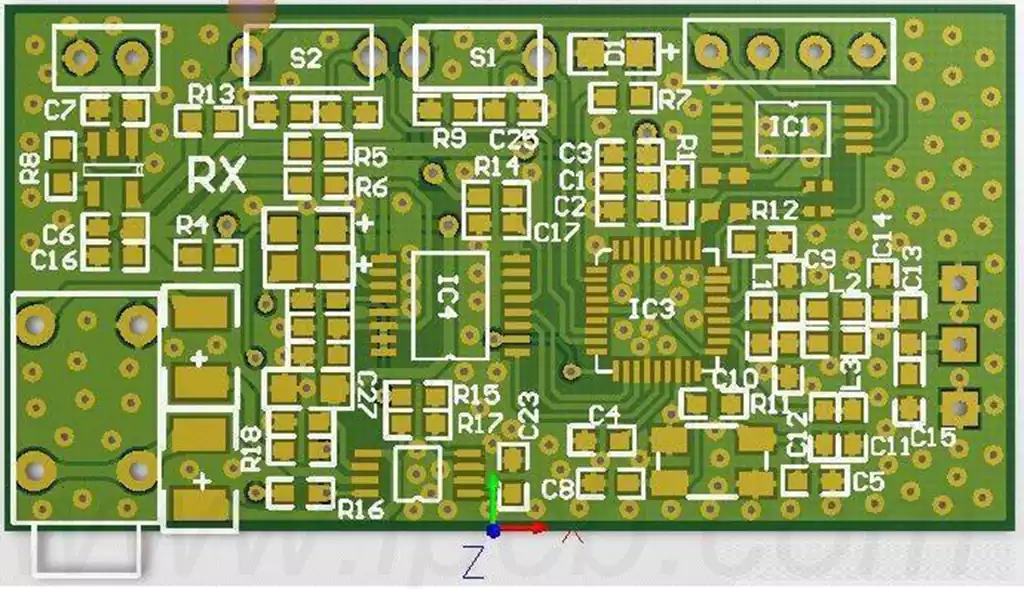
Methods for evaluating the effectiveness of electrical connections between layers when designing RF PCB stackup:
1.Importance of Electrical Connection
In RF PCB design, the effectiveness of electrical connections between layers directly affects the quality of signal transmission. Poor electrical connections may lead to signal attenuation, increased reflections and distortion, which in turn affects RF performance. Optimizing the connection between layers through reasonable design can maximize the efficiency and reliability of the circuit.
2.Laminated Structure Design
When designing RF PCB, the design of the laminated structure should fully consider the coupling characteristics between the conductors. Usually, a multi-layer structure is used to improve the stability of signal transmission. In the layer stacking design, the reasonable arrangement of the signal layer, ground layer and power supply layer will directly affect the electrical characteristics between the layers and the integrity of the signal. Ensure that the signal alignment is reasonably arranged with the reference ground, which can both reduce electromagnetic interference and improve the interference degree of the signal.
3.Consider interlayer insulation and dielectric materials
In the RF PCB design process, the choice of interlayer insulation and dielectric materials is another key factor affecting the effectiveness of the electrical connection. Different dielectric materials will affect the signal propagation speed and attenuation. Therefore, during design, the appropriate material needs to be selected according to the specific RF application requirements to ensure efficient signal transmission. Suitable materials can also reduce dielectric losses and improve the stability of electrical connections.
4.Design Rule Check (DRC)
During the layout and routing process, the implementation of Design Rule Checking (DRC) is an effective means to ensure that the electrical connections between the layers are effective.DRC identifies potential design errors, such as small spacing or improper thickness settings, and ensures that each parameter complies with the electrical and mechanical requirements, reducing the rate of defects in the later stages of production. Continuous checking ensures the reliability of electrical connections and improves the performance of the entire circuit.
5.Simulation and Testing
After completing the RF PCB design, it is very necessary to evaluate the effect of the electrical connection between the layers through simulation tools and actual testing. The use of high-frequency circuit simulation software, you can predict the signal behavior at the design stage, and targeted optimization of the design. In addition, physical testing can provide real-world connection performance data, helping to identify problems that may have been overlooked in the design and lead to improvements.
RF PCB stackup design requires not only reasonable material selection, but also attention to signal transmission stability and interference reduction. By following design principles and conducting system evaluations, designers can effectively improve circuit performance and reliability. Looking ahead, RF PCB design will continue to evolve as the demand for high-frequency devices continues to grow, providing important support for the high performance and stability of electronic products.
