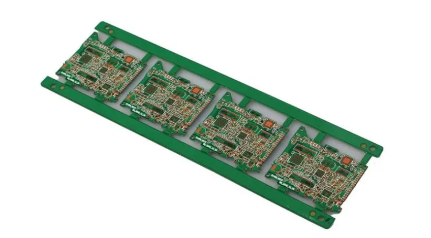
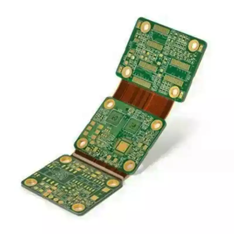
Transparent PCBs are circuit boards manufactured using transparent substrates (such as glass, polyimide or plastic) and transparent conductive materials (such as ITO or silver nanowires), combining electrical conductivity with light transmission. They find extensive application in flexible displays, smart touchscreens and medical devices. Within this manufacturing process, metal masks particularly high-precision laser-cut masks—play a critical role.
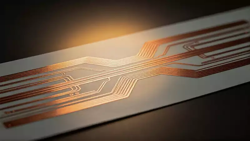
Metal stencils are primarily employed in the patterning process for the conductive layers of transparent PCBs. During the sputtering or evaporation of materials like ITO, precision laser-cut stencils made from stainless steel or nickel alloys cover non-circuit areas. This ensures precise deposition of the conductive material, forming micrometre-scale circuit patterns (e.g., 20μm line widths). Furthermore, during screen printing of conductive inks, metal masks can replace traditional stencils, enhancing printing precision on flexible transparent substrates (such as PET). This makes them suitable for small-batch, high-demand scenarios.
Compared to photoresist masks, metal masks offer significant advantages: Firstly, they are highly durable and reusable, making them suitable for mass production. Secondly, they exhibit resistance to high temperatures and chemical corrosion, adapting well to complex process environments. Thirdly, precision laser cutting technology enables higher accuracy, achieving ±10μm precision at 20μm line widths, meeting the design requirements for fine circuitry in transparent PCBs.
Principle of Operation for Metal Masks
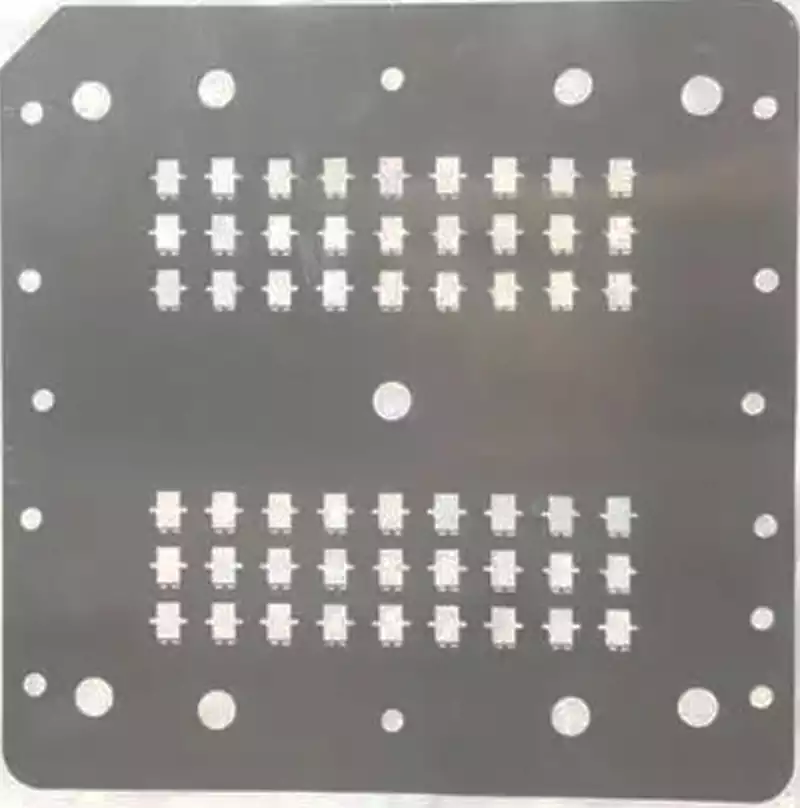
Metal masks are high-precision metal foils, typically fabricated from stainless steel or nickel alloys. Their surfaces feature micron-level intricate patterns formed via laser or chemical etching processes. Their primary function within electronics manufacturing is to precisely block patterns, enabling accurate deposition or etching of materials such as metals, phosphors, or conductive pastes.
- Key Role in Pattern Transfer
In OLED and MicroLED display manufacturing, the Fine Metal Mask (FMM) is positioned between the substrate and the evaporation source. When materials (such as organic light-emitting compounds) are evaporated at high temperatures, the mask’s apertures permit precise deposition onto the substrate, forming the required pixel array. - High-Precision Etching Technology
Advanced laser etching and electroforming processes ensure aperture precision within ±1μm, meeting the manufacturing demands of high-resolution display panels. - Tension Control and Reusability
Metal masks require exceptional flatness and deformation resistance. Through specialised heat treatment and tension regulation techniques, Zolida ensures stable pattern accuracy even after multiple uses.
Significant Advantages of Metal Masks
High Precision: Laser cutting technology guarantees ±10μm accuracy for metal masks, critical for manufacturing micro-sensors and similar devices. This precision ensures component stability and reliability, enhancing overall product performance.
Durability: Typically crafted from high-temperature resistant, corrosion-resistant materials like stainless steel or nickel alloys, metal masks can withstand over ten thousand reuses. This substantially reduces unit costs and boosts production efficiency.
Environmental Sustainability: Metal mask plates employ dry processing techniques during fabrication, minimising waste from chemical effluents and precious metals. This aligns with green manufacturing trends, supporting environmental conservation and sustainable development.
Leveraging their precision, exceptional durability, and eco-friendly advantages, metal mask plates precisely empower transparent PCB manufacturing. They propel electronic components towards miniaturisation and greater integration, laying a robust foundation for innovation in smart devices.