What is chip packaging? Chip packaging involves securing a bare die onto a specific substrate through a series of intricate processes, such as dicing, cleaning, bonding, wire bonding or flip-chip soldering. The die is then encapsulated using plastic materials (such as epoxy resin) while leads or solder balls are exposed to facilitate connection with external circuits.
During manufacturing, chips must be produced under strictly controlled conditions to prevent damage from environmental factors like temperature, humidity, and dust. However, real-world environments are far from ideal, with temperatures ranging from -40°C to 60°C, humidity potentially reaching 100%, and automotive products operating at temperatures exceeding 120°C. Consequently, chip packaging is crucial for ic, providing essential protection to ensure stable operation under diverse harsh conditions.
Protective Function
One primary role of encapsulation is shielding semiconductor chips from physical and chemical damage. It effectively isolates airborne contaminants, preventing circuit corrosion and subsequent degradation of electrical performance. Furthermore, encapsulation safeguards the chip surface and interconnections, shielding the fragile semiconductor from environmental hazards including mechanical stress, moisture, dust, and electrostatic discharge. Encapsulation materials like epoxy moulding compounds seal the chip and components, creating an optimal operating environment.
Support Function
The package provides mechanical support, securing the chip for circuit connections. Upon completion, it forms a specific profile that bolsters the entire device, enhancing durability and resistance to damage. The die pad serves to bear the chip, while epoxy adhesive bonds the chip to the pad. The pins also contribute to the overall structural support of the device.
Interconnection Function
The package ensures the interconnection between the chip’s electrodes and external circuits, enabling the transmission of signals and power. Pins and gold wires work in tandem to guarantee stable connections between the chip and external circuits, with pins connecting to external circuits and gold wires linking pins to the chip’s internal circuitry. The stability and reliability of this connection directly impact the device’s overall performance.
Reliability and Materials/Processing
The reliability of the package is a key metric for evaluating its performance. The selection of packaging materials (such as interconnect materials, substrate materials, and sealing materials) and processing techniques directly determines the chip’s operational lifespan and long-term stability under various environmental conditions. For instance, moisture can cause the ‘popcorn effect’ and electrochemical migration within the package, leading to device failure. Epoxy adhesives play a pivotal role in encapsulation, offering not only high bonding strength, thermal resistance, and sealing properties but also providing stable physical support. This reduces stress on the chip caused by temperature fluctuations, thereby minimising the risk of damage or failure. The plastic moulding compound protects the chip and bond wires from mechanical damage and moisture ingress.
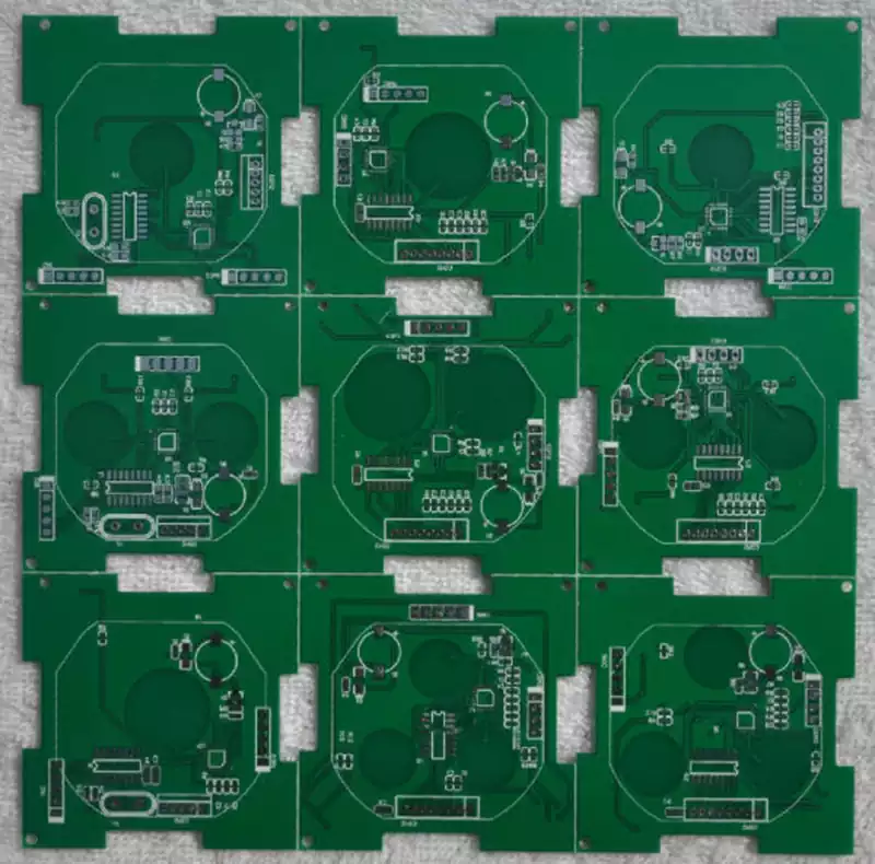
The chip packaging process flow can be divided into front-end operations (pre-moulding) and back-end operations (post-moulding). The core difference between the two lies in the environmental cleanliness requirements (front-end requires Class 100 cleanrooms, while back-end can be relaxed to Class 10,000).
Front-end Operations: Die-Level Processing
- Wafer Thinning: Reduces wafer thickness from 700μm to 50-200μm via grinding or chemical mechanical polishing (CMP), lowering thermal resistance and facilitating dicing.
- Wafer Dicing: Separates wafers into individual dies (chips) using laser or diamond blades along predetermined paths, maintaining dimensional accuracy within ±5μm.
- Die Attach: Secures the die to the substrate using conductive adhesive or solder, establishing mechanical connection and initial thermal pathways.
- Chip Interconnection (Wire Bonding/Flip Chip)
Wire Bonding: Connects chip pads to substrate pins using gold/copper wires, suitable for medium-to-low pin density applications;
Flip Chip Bonding: Directly connects chip electrode bumps to substrate pads, shortening signal paths and enhancing high-frequency performance.
Back-end Operations: Packaging Formation and Testing
- Moulding techniques employ processes such as injection moulding and potting to encapsulate the chip within plastic or ceramic materials, forming the package. Plastic packaging (e.g., EMC epoxy moulding compounds) offers low cost and high efficiency, commanding over 90% market share; ceramic packaging (e.g., Al₂O₃) provides high-temperature resistance and superior thermal dissipation, used in military and automotive electronics.
- Trimming and die-cutting processes remove excess material from the moulded package and sever the metal lead frame connecting the pins, forming individual leads.
- Soldering and marking involve tin-plating the leads to enhance solderability, while laser marking imprints product information (model, batch, etc.).
- Testing and sorting utilise ATE equipment to verify electrical performance, grading products by yield rate.
Chip packaging technology constitutes a critical stage in semiconductor manufacturing, essential for ensuring stable and reliable chip operation across diverse electronic devices. With the continuous advancement of microelectronics and integrated circuit technology, chip packaging has been propelled to the forefront of technological evolution as Moore’s Law approaches its physical limits. Confronted with challenges of size, density, power, cost, and reliability, packaging technology continues to innovate, evolving from basic protective functions towards integrated system-level solutions that synergise electrical, thermal, signal, and sealing functions.
Advanced chip packaging techniques, such as 2.5D and 3D packaging, achieve greater assembly density and efficiency while driving the convergence of chiplet technology and heterogeneous integration to optimise system performance and cost-effectiveness. Future packaging technologies will continue to achieve breakthroughs in material innovation, process advancements, and AI-driven design tools to meet the demand for high-performance, low-power, and highly reliable chips in fields such as 5G communications, artificial intelligence, the Internet of Things, and automotive electronics.
