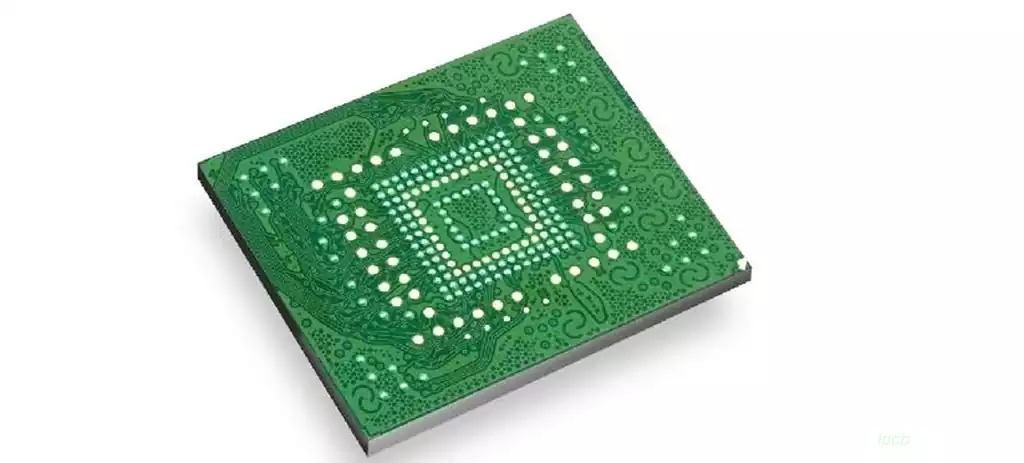
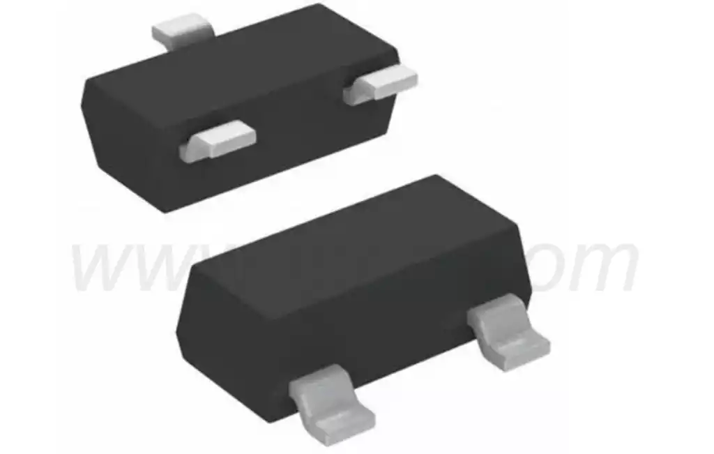
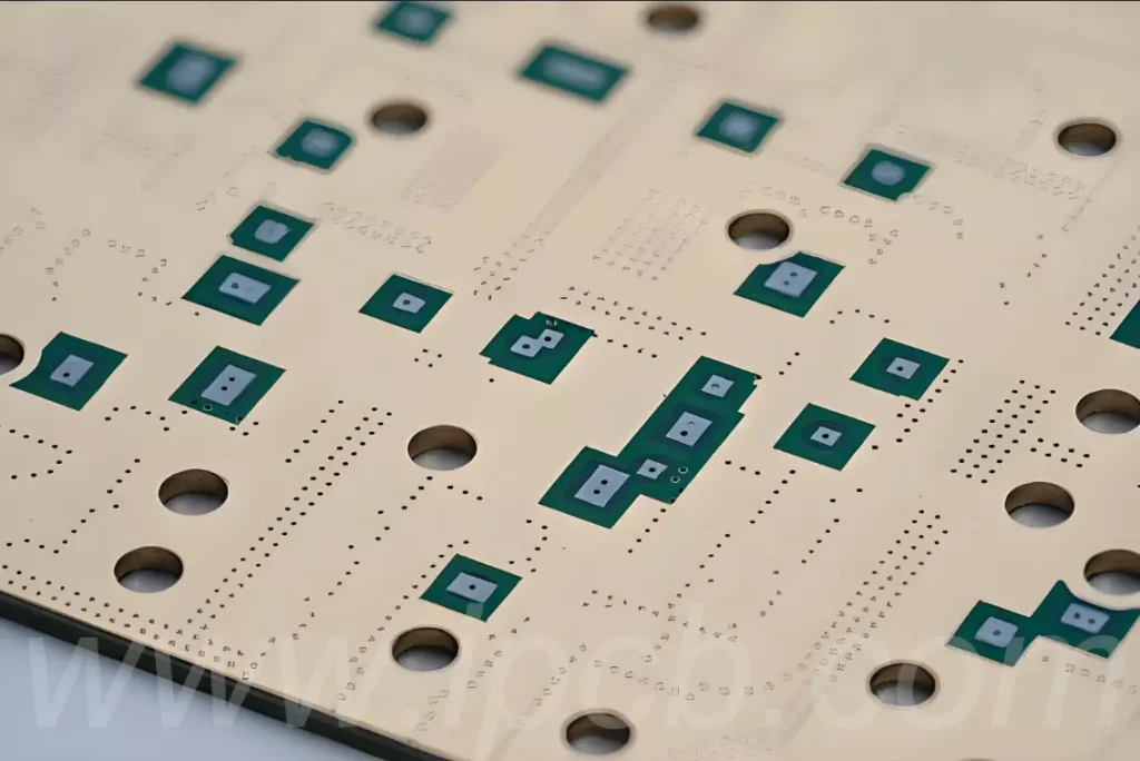
The precision of ceramic circuit board design directly determines product reliability and mass production yield rates. Compared to traditional FR4 circuit boards, ceramic circuit board (such as aluminium oxide and aluminium nitride) exhibit brittle-hard characteristics, unique thermal expansion coefficients, and specific process compatibility requirements. Many engineers, either adhering to conventional design thinking or overlooking the distinct properties of ceramic materials, introduce latent issues during the design phase. This ultimately leads to batch failures, soaring costs, and delivery delays. These pitfalls are not insurmountable; the key lies in precisely matching ceramic material properties with design specifications.This article focuses on five common pitfalls engineers most frequently encounter, using practical case studies to deconstruct avoidance strategies and facilitate the design of highly reliable, easily mass-producible ceramic circuit boards.
1.One-size-fits-all substrate selection: Mismatched performance and application scenarios
Substrate selection marks the initial step in ceramic circuit board design, yet represents the most common pitfall. Many engineers default to aluminium oxide (Al₂O₃) ceramics or blindly pursue high thermal conductivity by selecting aluminium nitride (AlN), overlooking core application requirements. This leads to either over-engineered performance or compromised reliability.
Different ceramic circuit boards exhibit significant performance variations, each suited to distinct scenarios: Aluminium oxide ceramics offer lower cost and excellent insulation, but with a thermal conductivity of merely 20-30 W/(m·K), they are best suited for low-to-medium power, cost-sensitive applications (e.g., domestic LED driver modules); Aluminium nitride ceramics achieve thermal conductivities of 180–200 W/(m·K), approaching metallic levels, yet their high cost and complex processing restrict their use to high-power, high-temperature applications (e.g., new energy vehicle inverters, aerospace power modules). Employing alumina ceramics in high-power scenarios risks chip overheating and burnout due to inadequate heat dissipation, shortening product lifespan; Employing aluminium nitride ceramics in standard low-power applications would increase unit costs by 3-5 times, constituting a waste of resources.
When formulating mitigation strategies, ‘scenario-specific matching’ must be the core principle to ensure selected materials and designs perfectly align with practical requirements. Specifically, three core product metrics must first be defined: power density, operating temperature, and cost budget. These factors directly determine subsequent material selection.
For medium-to-low power applications (≤50W) operating at ambient temperatures, alumina ceramics are undoubtedly the preferred material. Renowned for their outstanding cost-effectiveness and reliability, alumina ceramics are widely adopted in this power range. They not only meet fundamental electrical performance requirements but also excel in cost control, making them an ideal choice for economically efficient solutions.
However, when applications shift to high power (power > 100W) and high temperatures (temperature > 150°C), alumina ceramics become inadequate. This is where aluminium nitride ceramics come into their own, emerging as the preferred material for high-power, high-temperature environments. Aluminium nitride ceramics possess outstanding thermal conductivity and high-temperature resistance, effectively addressing heat accumulation issues caused by high power. To further enhance heat dissipation, pairing with a copper-clad layer ≥2oz is recommended. This significantly improves thermal efficiency, ensuring the stability and reliability of equipment during high-power operation.
In specialised high-frequency applications, materials face heightened demands regarding dielectric properties. Here, beryllium oxide (BeO) ceramics distinguish themselves through exceptionally low dielectric loss, establishing them as the ideal choice for high-frequency domains. However, the toxicity of beryllium oxide ceramics warrants serious attention. Strict adherence to safety protocols during processing and handling is imperative, alongside comprehensive toxicological protection measures to safeguard personnel.
2.Thermal design imbalance, neglecting the thermal properties of ceramic materials
Common thermal design pitfalls for ceramic circuit boards centre on two primary issues: ‘overlooking thermal expansion differences’ and ‘inadequate heat dissipation structure design’. Ceramic materials exhibit a thermal expansion coefficient significantly lower than metals (e.g., alumina CTE ~7×10⁻⁶/℃, copper CTE ~17×10⁻⁶/℃), coupled with high brittleness and poor thermal shock resistance. Improper thermal design readily leads to failures such as interlayer delamination, substrate cracking, and solder joint detachment.
Common design errors include: failing to incorporate thermal expansion compensation space, rigidly bonding ceramic circuit boards to metal casings, which generates stresses during thermal cycling due to differing expansion/contraction rates, leading to edge cracking; poorly positioned heat dissipation holes concentrated in non-critical heat-generating areas, or holes being excessively small (<0.5mm), impairing heat conduction; failure to optimise copper layer distribution, resulting in insufficient thickness over core heat-generating zones and impaired heat diffusion. A new energy vehicle power module project experienced initial production yields below 60% due to these issues. Investigation revealed rigid bonding between ceramic circuit board and metal baseplate, coupled with core-zone copper layers of merely 1oz, incapable of withstanding high-temperature stresses and thermal loads.
Mitigation requires a dual-pronged approach: Firstly, optimise thermal expansion compatibility by replacing rigid connections with elastic ones (e.g., silicone spacers, thermal conductive adhesives) to buffer stresses from thermal cycling. For core heat zones, employ ‘thickened copper foil + grid layout’ – increasing copper thickness to 2-3 oz and controlling grid spacing at 0.8-1.2mm to enhance both heat dissipation and stress distribution. Concurrently, scientifically design thermal structures by incorporating heat dissipation holes (≥1mm diameter) beneath core heat-generating zones, with copper-plated walls to enhance thermal conductivity. For extremely high power applications, employ embedded thermal channels by reserving heat-conductive holes within ceramic substrates, filled with high-thermal-conductivity materials (e.g., copper powder, graphene) to boost dissipation efficiency by over 30%. Concurrently, thermal simulation tools must validate the design to ensure the surface temperature differential across the substrate remains ≤20℃ under operating conditions.
3.Haphazard circuit layout disregarding ceramic processing characteristics
Another common high-frequency pitfall involves applying FR4 circuit board layout principles to ceramic circuit boards. Ceramic materials are brittle and rigid, demanding high machining precision. Improper details such as trace width, spacing, and via design can increase manufacturing complexity, cause scrap rates to soar, and even compromise electrical performance.
Specific errors include: – Excessively narrow trace widths (<0.2mm) risk trace fractures during ceramic circuit board etching and compromise current-carrying capacity; – Insufficient trace spacing (<0.3mm) predisposes to tracking breakdown under high-voltage conditions, with heightened risk in humid environments; Excessive via count or undersized via diameter (<0.3mm) may cause chipping and cracking during ceramic drilling, complicate via filling, and compromise interlayer interconnect reliability. Designing circuit corners as right angles concentrates stress during current flow while increasing etching complexity.
Mitigation strategies must align with ceramic processing characteristics and electrical requirements: – Circuit design: Standard trace width ≥0.3mm; traces carrying high currents (>5A) ≥0.8mm; trace spacing ≥0.5mm. For high-voltage applications (>1kV), spacing must be further increased to 1.0-1.5mm to mitigate tracking risks. For via design, hole diameters should be controlled between 0.5–1.0mm, with quantities minimised as required. Maintain a distance of ≥1.5mm between via edges and substrate edges to prevent edge chipping. Prioritise conductive paste or copper paste for via filling to ensure stable interlayer interconnections. Implement 45° chamfers or rounded transitions (with a radius ≥0.2mm) at circuit corners to reduce stress concentration and etching inaccuracies. Additionally, layout must incorporate machining reference holes (2-3mm diameter), positioned ≥2mm from traces to prevent damage during processing.
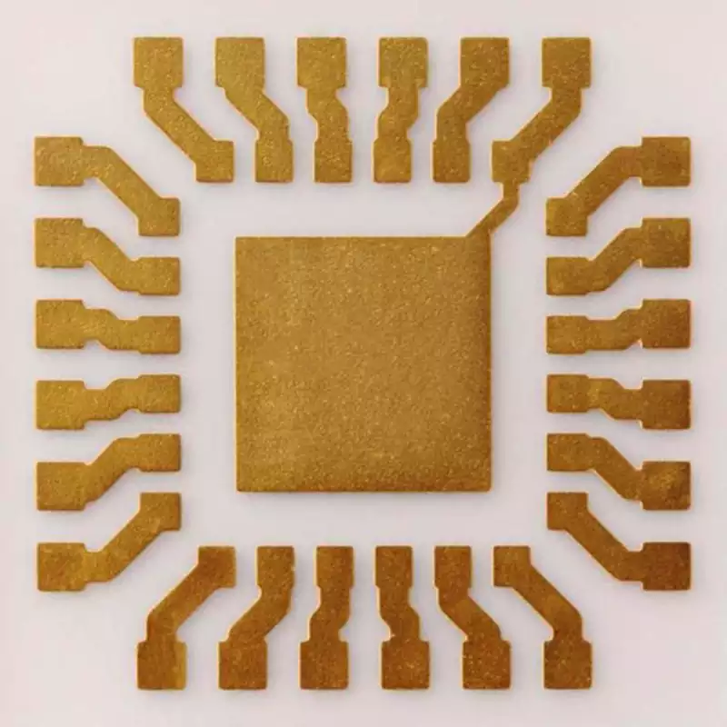
4.Disconnected packaging and assembly design, insufficient compatibility
Neglecting compatibility between ceramic circuit boards and packaging/assembly processes during design leads to subsequent assembly difficulties and reduced reliability – a pitfall often overlooked by engineers. The brittleness and dimensional precision requirements of ceramic substrates impose stringent constraints on packaging methods, assembly pressures, and fixation techniques, representing a significant departure from the assembly logic of traditional FR4 circuit boards.
Common issues include: mismatched packaging dimensions with the ceramic circuit board, insufficient tolerance allowance (<0.1mm), leading to mechanical stresses during assembly that cause substrate cracking; Utilising snap-fit fasteners concentrates clamping pressure at substrate edges, causing edge chipping as ceramic material cannot withstand localised stress; Inappropriate soldering process selection, such as employing high-temperature solder paste (melting point >260°C), exceeding ceramic substrates’ thermal endurance limits (most ceramic substrates have long-term thermal resistance ≤220°C), resulting in substrate deformation and interlayer delamination; Unreasonable pin layout causes uneven stress distribution during assembly, resulting in ceramic substrate cracking due to pin tension.
Mitigation requires ‘design and assembly process coordination’: Dimensional tolerances should be designed with a 0.15-0.2mm fit tolerance between ceramic substrate and housing, allowing sufficient assembly clearance. Screw fastening (with evenly spaced screws) should be prioritised, combined with silicone spacers to distribute pressure and prevent localised stress concentration. For soldering, employ medium-temperature solder paste (melting point 180-220°C) with a soldering time controlled at 10-15 seconds to prevent prolonged high-temperature heating. Adopt a symmetrical pin layout with uniform pin lengths to minimise uneven stress during assembly. Furthermore, design teams must liaise proactively with packaging and assembly teams to clarify process parameters, ensuring the design solution aligns with mass production assembly workflows.
5.Neglecting process compatibility and insufficient mass production feasibility
Some engineers excessively prioritise performance during design while overlooking the process compatibility of ceramic circuit boards. This results in designs that cannot be mass-produced, or face extremely low yield rates and uncontrollable costs during production. The manufacturing processes for ceramic circuit boards (such as sintering, etching, and copper plating) are significantly more complex than those for FR4. Design solutions must align with process capabilities; otherwise, they will fall into the predicament of being ‘feasible on paper but difficult to mass-produce’.
Common pitfalls include: – Demanding excessively high interlayer alignment precision (<5μm) for multilayer ceramic circuit boards, exceeding conventional equipment limits (typically 8-10μm), resulting in interlayer shorts and interconnect failures; – Selecting specialised copper plating processes (e.g., thick copper plating >5oz) without considering factory capabilities, leading to uneven plating and copper layer delamination; Designing complex embedded structures while neglecting the shrinkage characteristics of the sintering process, resulting in excessive dimensional deviations in the finished product that prevent compatibility with subsequent assembly. One high-end ceramic circuit board project encountered difficulties due to a design requiring three layers with alignment accuracy ≤3μm, which most domestic factories were unable to process. Ultimately, the project had to be outsourced to an overseas manufacturer, doubling the cost and extending the delivery cycle to three months.
Mitigation strategies must prioritise ‘mass production feasibility’: Prior to design, thoroughly investigate partner factories’ process capabilities, clarifying core parameters such as machining precision, copper plating thickness, and sintering shrinkage rate. Control design specifications within process limits (e.g., interlayer alignment accuracy ≥8μm, copper plating thickness ≤3oz). When designing multilayer structures, incorporate compensation for sintering shrinkage (typically 2-3%) and adjust dimensions based on the factory’s actual sintering data. Avoid overly complex special structures; if necessary, produce samples in advance to validate process feasibility. Additionally, select mature manufacturing processes (such as DBC direct copper-clad laminate or LTCC low-temperature co-fired ceramic) to replace niche, complex techniques, thereby improving mass production yield and reducing costs.
Avoiding pitfalls in ceramic circuit board design fundamentally involves achieving precise alignment between material properties, design solutions, manufacturing capabilities, and application scenarios. Engineers must transcend conventional PCB design paradigms, fully recognising ceramic materials’ inherent brittleness, unique thermal expansion characteristics, and stringent machining precision requirements. Rigorous control across five dimensions—substrate selection, thermal design, circuit layout, packaging/assembly, and process compatibility—is essential. This approach simultaneously avoids high-frequency pitfalls while balancing performance with mass-production feasibility.
Every detail optimised during the design phase contributes to cost reduction and enhanced reliability in subsequent mass production. As ceramic circuit boards gain wider adoption in high-end electronics, design specifications will become increasingly refined. Only by grounding designs in practical requirements, respecting material properties, and collaborating with manufacturing capabilities can ceramic circuit board products be engineered that deliver reliability, cost-effectiveness, and mass-production viability.
