The Fundamental Relationship Between Dielectric Constant and Capacitance in PCB Design
In electronic circuit design, the relationship between dielectric constant and capacitance is one of the fundamental concepts for understanding signal transmission and circuit stability. For PCB engineers, these two parameters not only affect the electrical characteristics of the circuit but also directly relate to high-speed signal integrity, impedance control, and power integrity design.
Dielectric constant, usually represented by Dk or εr, describes a material’s ability to store electrical energy in an electric field. Simply put, the higher the dielectric constant, the greater the material’s influence on the electric field, meaning that electrical signals propagate more slowly within the material. In PCB manufacturing, common substrates such as FR-4, PTFE, or ceramic-filled materials each have their own distinct dielectric constants.
Capacitance, on the other hand, represents the ability to store charge between two conductors. When an insulating medium exists between two conductors, a capacitor structure is formed. In PCBs, this structure is almost ubiquitous, for example:
between signal lines
between signal layers and ground planes
between power layers and ground planes
parasitic capacitance between adjacent conductors
In an ideal model, capacitance is determined by several factors: conductor area, conductor spacing, and the dielectric constant of the dielectric material. The dielectric constant is one of the most important factors determining PCB parasitic capacitance. As the dielectric constant of the material increases, the capacitance value formed under the same structure also increases accordingly.
This relationship is particularly critical in high-speed circuit design. For example, in high-speed digital interfaces or RF circuits, the dielectric constant of the PCB material not only affects signal propagation speed but also changes the characteristic impedance of the line, thus affecting the signal integrity of the entire system.
Therefore, in modern PCB engineering, understanding the relationship between dielectric constant and capacitance is a crucial foundation for high-speed design, impedance control, and material selection.
How Capacitors Are Formed in PCB Structures
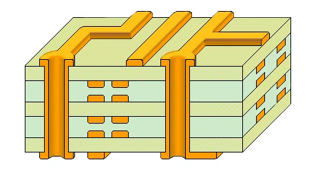
In PCB circuit boards, capacitance is not only found in specially designed capacitor components. In fact, a capacitor structure is formed whenever there is an insulating medium between two conductors. Therefore, a significant amount of parasitic capacitance naturally occurs within a PCB, which is a crucial factor affecting circuit performance.
The most typical capacitor structure appears between a signal line and a reference plane. When a signal line is routed on a PCB surface or inner layer, and a complete ground or power layer exists beneath it, a structure similar to a parallel-plate capacitor is formed. The signal line acts as one pole of the capacitor, the reference plane as the other, and the PCB substrate (e.g., FR-4) in between acts as the dielectric material.
This structure is very common in high-speed circuits. For example, in microstrip or stripline structures, the capacitance between the signal line and the reference layer directly affects the characteristic impedance of the line. When parasitic capacitance increases, the line impedance typically decreases, thus altering signal transmission characteristics.
Besides the area between the signal line and the reference plane, several other situations in a PCB can generate capacitance, including:
First, coupling capacitance between signal lines.
When two traces are close together, their electric fields influence each other, forming coupling capacitance. This type of capacitance can cause crosstalk, which is particularly noticeable in high-speed digital circuits.
Second, planar capacitance between power and ground layers.
In multilayer PCBs, a large planar capacitance forms between the power and ground layers. This capacitance helps with power decoupling and improves power integrity to some extent, and is therefore sometimes considered a type of “distributed capacitance.”
Third, parasitic capacitance generated by via structures.
In multilayer PCBs, vias connect conductors on different layers. When a via is close to a reference plane, it also forms a certain amount of parasitic capacitance, which requires special attention in high-speed signal design.
The size of the capacitance is generally affected by the following three factors:
Area between conductors
Distance between conductors
Dielectric constant of the dielectric material
Among these, the dielectric constant is one of the important parameters of PCB materials. When the dielectric constant of the material is higher, the capacitance formed under the same structure will be larger. Therefore, in high-speed or RF circuit design, engineers often choose materials with lower dielectric constants to reduce the impact of parasitic capacitance on signal transmission.
Understanding the formation mechanism of capacitance within a PCB not only helps optimize circuit layout but also allows engineers to control electrical performance in advance during material selection and layer stack-up design, thereby improving the stability and reliability of the entire system.
Differences in Dielectric Constants of Different PCB Materials
In PCB design and manufacturing, the choice of substrate has a significant impact on electrical performance. Among these, the dielectric constant of the material is one of the key parameters that engineers must consider when designing high-speed circuits. Differences in the dielectric constant of different PCB materials directly affect signal propagation speed, impedance control, and the size of parasitic capacitance.
The most common PCB substrate is FR-4. FR-4 is a composite material composed of glass fiber and epoxy resin, which has advantages such as low cost, high mechanical strength, and mature manufacturing, and is therefore widely used in most electronic products. Generally, the dielectric constant of FR-4 is approximately between 4.2 and 4.8, although the specific value will vary depending on the frequency, material formulation, and manufacturing process.
In high-speed digital circuits or radio frequency applications, engineers typically choose materials with lower dielectric constants and higher stability. For example, some high-frequency copper-clad laminate (CCL) materials use PTFE (polytetrafluoroethylene) or ceramic filler technology, with a dielectric constant typically between 2.2 and 3.5. These materials can significantly reduce signal delay and high-frequency signal loss, and are therefore commonly used in 5G communications, radar systems, and high-speed network equipment.
Besides FR-4 and high-frequency materials, there are also intermediate-performance PCB materials, such as modified epoxy resins or low-loss resin systems. These materials strike a balance between cost and performance, making them suitable for data communication equipment, server motherboards, and high-speed consumer electronics.
It is worth noting that the dielectric constant of a material not only affects signal propagation speed but also changes the characteristic impedance of PCB traces. When the dielectric constant is high, the impedance of the traces under the same structure is usually lower; conversely, when the dielectric constant is low, the impedance is relatively higher. Therefore, when designing impedance control, engineers must consider multiple factors simultaneously, including material parameters, trace width, and dielectric thickness.
Furthermore, the dielectric constant also fluctuates to some extent with frequency changes; this phenomenon is called “dielectric dispersion.” In high-frequency or high-speed applications, insufficient dielectric constant stability of materials can lead to inconsistent signal propagation characteristics, thus affecting the overall system performance.
Therefore, when selecting PCB materials, it is necessary to consider not only cost and processing performance but also a comprehensive evaluation based on circuit operating frequency and signal integrity requirements. Appropriate material selection can effectively control parasitic capacitance, improve signal transmission quality, and provide a more stable foundation for subsequent impedance design.
How Dielectric Constant Affects Signal Integrity and Impedance Control in High-Speed PCBs
As electronic products evolve towards higher speeds and frequencies, the impact of the dielectric constant of PCB materials on circuit performance becomes increasingly significant. In high-speed digital circuits and radio frequency systems, signal propagation depends not only on the conductor itself but also on the electrical characteristics of the surrounding dielectric material. Therefore, understanding how the dielectric constant affects signal integrity and impedance control is a crucial aspect of modern PCB design.
First, the dielectric constant directly affects signal propagation speed. In PCBs, the propagation speed of electrical signals is inversely proportional to the dielectric constant of the dielectric material. Generally, the higher the dielectric constant, the slower the signal propagates within that material. This means that in high-speed interfaces (such as high-speed data communication or RF circuits), using materials with high dielectric constants may increase signal delay, thus affecting the timing stability of the system.
Secondly, dielectric constant is one of the important parameters determining the characteristic impedance of a line. In microstrip or stripline structures, line impedance depends not only on the trace width and dielectric thickness but also closely on the dielectric constant of the material. When the dielectric constant increases, the characteristic impedance of the line typically decreases. Therefore, when designing impedance control, engineers must adjust trace dimensions according to the dielectric constant of the selected material to ensure the stability of signal transmission.
Thirdly, dielectric constant also affects parasitic capacitance and signal coupling. In PCB structures, parasitic capacitances are formed between adjacent traces and between signal layers and reference layers. If the dielectric constant of the material is high, these parasitic capacitances will increase, potentially leading to signal crosstalk or high-frequency loss. In high-speed circuit design, excessive parasitic capacitance can reduce signal edge speed and even affect the reliability of data transmission.
Furthermore, the stability of the dielectric constant of the material is also crucial in high-frequency applications. If the dielectric constant changes significantly with frequency or temperature, it can lead to impedance shifts in the circuit, thus affecting the overall system performance. Therefore, in RF communication, 5G equipment, or high-speed network systems, specialized high-frequency materials with more stable dielectric constants are typically chosen.
In summary, the dielectric constant is not only a fundamental parameter of PCB materials but also a crucial factor affecting signal integrity, impedance matching, and system performance. In practical design, by appropriately selecting materials and optimizing the circuit structure, parasitic capacitance can be effectively controlled, signal transmission quality improved, and stable circuit operation ensured in high-speed environments.
Summary
Understanding the Importance of the Relationship Between Dielectric Constant and Capacitance in PCB Design
In the PCB design and manufacturing process, the relationship between dielectric constant and capacitance is one of the fundamental factors affecting circuit performance. Since the PCB structure itself is composed of conductors and dielectric materials, a capacitive structure is naturally formed as long as there is an insulating layer between the conductors. Therefore, the dielectric constant of the PCB material directly affects the size of parasitic capacitance, thereby affecting signal transmission characteristics.
This effect is particularly pronounced in high-speed digital circuits and RF systems. A higher dielectric constant typically increases parasitic capacitance and reduces signal propagation speed, while a lower dielectric constant helps reduce signal delay and improve transmission efficiency. Therefore, in high-speed PCB design, engineers need to consider not only circuit structure and layer stack-up but also the appropriate selection of materials to ensure impedance control and signal integrity meet system requirements.
Furthermore, the stability of the material’s dielectric constant is crucial. Significant changes in material parameters under different frequencies or temperatures can lead to impedance shifts or signal distortion, affecting overall circuit performance. Therefore, in high-frequency communications, data center equipment, and high-speed interface applications, material selection is often a critical decision during the design phase.
Overall, a deep understanding of the relationship between dielectric constant and capacitance can help engineers better optimize PCB structure design, reduce parasitic effects, and improve the overall stability and reliability of the system.