The Multidimensional Composition of Flex PCB Thickness: Beyond the Definition of “Board Material”
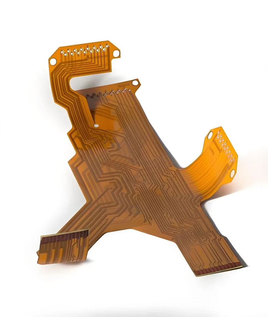
When we talk about flex PCB thickness, we are dealing with a dynamic, multi-material composite system.
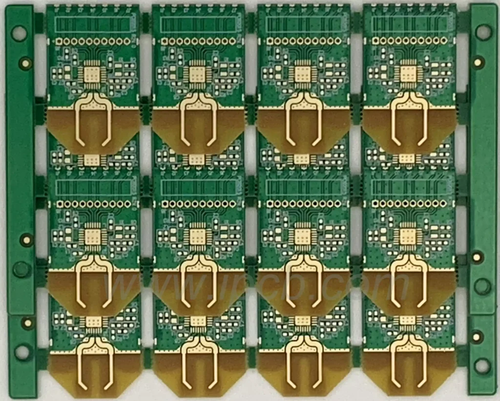
Unlike the single-board concept of rigid FR4, the thickness of a flexible circuit board (FPC) is precisely composed of multiple functional layers, and every micrometer increase or decrease directly alters the circuit’s “mechanical lifespan.”
The Core of Base Film Thickness
The core of an FPC is typically polyimide (PI).
Common Specifications: The most mainstream PI film thicknesses are 12.5μm (0.5 mil) and 25μm (1 mil). Thinner 7.5μm films are also available for applications with extremely limited space requirements.
Physical Properties: The PI film not only provides insulation but also determines the circuit’s tensile strength. Thickness selection must consider chemical resistance, as thinner PI films are highly sensitive to tension during subsequent etching processes.
Adhesive vs. Adhesiveless Substrate: This is a key technological dividing line affecting the thickness of flex PCBs.
Adhesive-based substrate: Copper foil is pressed onto the PI using epoxy or acrylic adhesive. This typically adds an extra 12μm to 25μm of thickness. While less expensive, thickness tolerance is more difficult to control due to the high coefficient of thermal expansion (CTE) of the adhesive.
Adhesive-less substrate: Copper is directly deposited or sputtered onto the PI. This process not only significantly reduces the overall thickness (eliminating the adhesive layer) but also improves the circuit’s heat resistance and impedance control accuracy.
Copper Foil Thickness Contribution to FPC: Commonly used copper foils are rolled copper (RA Copper) and electrolytic copper (ED Copper).
1/3 oz (12μm) and 1/2 oz (18μm): These are the standard for achieving ultra-thin flexible circuits. The Impact of Thickness on Fatigue: While thicker copper foil increases current-carrying capacity, the stress on the copper foil surface, S = Et / 2r (where t is the thickness), increases linearly during dynamic bending, leading to earlier metal fatigue cracks.
Balancing Coverlay and Flexibility
If the substrate is the skeleton, the coverlay is the skin of the FPC. Coverlay thickness is often overlooked by non-experts when discussing flex PCB thickness, but in actual manufacturing, it is a decisive factor in bending performance.
Standard Coverlay Composition
A typical coverlay consists of a layer of PI and a layer of semi-cured adhesive.
Common Thickness Combination: 12.5μm PI + 15μm Adhesive.
Coverlay Loss: During vacuum bonding, the adhesive flows into the line gaps. This means that the measured thickness at the top of the lines will be slightly less than the sum of the nominal thicknesses; this “thickness depression” is a variable that must be compensated for in high-precision impedance calculations.
Alternatives to Flexible Solder Mask
In certain localized areas with extremely stringent thickness requirements (such as the hinge area of a foldable screen), we use photosensitive flexible solder mask instead of coverlay.
Thickness Advantage: Solder mask typically adds only 10-15μm of thickness.
Trade-off: While thinner, the flexural lifespan of solder mask is generally inferior to that of continuous PI film coverlay.
Local Thickening Strategy: Stiffener
One of the great advantages of FPC is its non-uniform thickness. By increasing the flex PCB thickness in specific areas, we can achieve a balance between rigidity and flexibility.
FR4 Stiffener
In areas where components need to be soldered, 0.2mm to 1.0mm of FR4 is typically laminated. This is not part of the board’s own lamination thickness, but it is an important component of the overall assembly thickness.
PI Stiffener and Stainless Steel Stiffener
PI Stiffener: Used to increase the thickness of the gold finger portion to accommodate ZIF connectors.
Stainless Steel Stiffener: Provides extremely strong physical support and heat dissipation capabilities, commonly found in VCM modules for cameras, with a thickness typically around 0.1mm.
Mathematical Model of Dynamic Bending and Thickness (Bending Radius Calculation)
In flexible circuit design, the flex PCB thickness directly determines the product’s “lifespan limit.” A common misconception is that as long as the material is soft, it can be bent indefinitely. In reality, bending performance is determined by the ratio of thickness to bending radius.
Bending Stress and Neutral Axis: When an FPC bends, the outer layer experiences tensile stress, and the inner layer experiences compressive stress. There is a plane in the middle that experiences neither tension nor compression, called the neutral plane.
Negative Effects of Thickness: As the total thickness $T$ increases, the distance of the outer copper foil from the neutral plane increases, and the stress it experiences increases exponentially.
If your flex PCB thickness is 0.12mm, then the dynamic bending radius needs to be at least 1.44mm.
Micron-level variables affecting dynamic lifespan: In high-end orders, customers often ask why lifespans differ even with the same thickness. Advantages of rolled copper (RA Copper): Although the thickness is the same as electrolytic copper, rolled copper has a lamellar crystal structure, and at the same thickness, its bending resistance is several times that of electrolytic copper.
Coverlay opening design: If the edge of the coverlay is located at a bending stress point, stress concentration will occur, leading to breakage at the abrupt thickness change.
Thickness challenges of multilayer FPCs and Rigid-Flex boards: When FPCs evolve from single-layer to multilayer, or are combined with FR4 to form rigid-flex boards, thickness management becomes a “spatial acrobatics.”
Air Gap Construction in Multilayer Flexible Boards: To increase the number of layers without sacrificing flexibility, we typically do not laminate all layers separately.
Structural Analysis: In the bending region, each FPC layer is independent (separate), with air gaps between layers.
Thickness Logic: Although the individual layer thickness remains unchanged, the “apparent thickness” increases. Because the layers can slide freely, bending resistance is greatly reduced.
Thickness Transition at Rigid-Flex Joints
In Rigid-Flex designs, the most vulnerable area is the interface between the rigid and flexible boards.
Adhesive Overflow Control: During lamination, the FPC adhesive flows into the rigid board area, forming a “fiberglass wetting zone.” If the thickness abruptly changes in this area, it can cause signal reflections at impedance discontinuities.
Strain Relief: Flexible adhesive is typically applied at the interface to create a slope in the thickness, preventing stress from vertically cutting the copper foil.
Impedance Control Implementation in Extremely Thin Materials
In 5G and high-speed transmission applications, even small fluctuations in flex PCB thickness can directly ruin signal quality.
The application of low-dielectric-constant (Low-Dk) materials: Due to the extremely thin nature of FPCs, very narrow linewidths are often required to achieve a 50Ω impedance.
Technical bottleneck: If the linewidth is narrower than 2mil, manufacturing yield drops sharply. Solution: Increase the dielectric layer thickness (using a thicker PI core) or select a low-Dk material. However, increasing the thickness compromises flexibility.
The impact of shielding on thickness: To address EMI issues, FPCs often use silver paste or black film shielding layers. Thickness contribution: This type of shielding layer adds only about 10um-15um of thickness on one side. Performance comparison: Compared to traditional copper foil shielding, this special shielding film provides excellent flexibility while maintaining an extremely thin thickness.
Cost, Yield, and Manufacturing Limits
Why is the pricing logic for FPCs completely different from FR4? Thickness tolerance is key.
Why is “thin” more expensive? In flexible PCB manufacturing, extremely thin materials (such as 12.5µm PI) are prone to curling and wrinkling due to tension when passing through chemical baths.
Equipment Costs: Specialized roll-to-roll production lines are required. Auxiliary Materials: Temporary carrier boards may need to be pasted at each process, significantly increasing labor and material costs.
Industry Standards for Thickness Tolerance: The thickness tolerance for rigid FR4 PCBs is typically ±10%, but for flex PCBs, due to the higher material compression ratio, the industry generally accepts ±0.03mm or even wider tolerances.
If customers require micron-level thickness control, “material selection and lamination” and “laser thickness measurement” are usually required, which are high-premium services.
Future Trends: Beyond the Thickness Limits of PI and New Materials
With the evolution of 6G communication and wearable medical devices, traditional polyimide (PI) is facing challenges in balancing thickness and dielectric loss.
The Rise of Liquid Crystal Polymers (LCPs): LCPs are becoming the new favorite for high-end flex PCB thickness management. Moisture Absorption and Stability: LCPs have extremely low moisture absorption (approximately 0.04%), meaning their thickness expansion is almost zero in humid environments, ensuring phase stability of high-frequency signals.
Multilayer Ultra-Thinning: LCPs can achieve single-layer stacks of 25µm or even thinner without adhesives, making ultra-thin flexible boards with more than 10 layers possible.
Embedded Components Technology: To further reduce overall thickness, the industry is starting to embed resistors, capacitors, and even ICs directly into the dielectric layer of the FPC. Space Compression: This technology eliminates the pad height required for surface mount technology (SMT), reducing the overall module thickness by more than 40%.
Challenges: Embedded designs require thickness tolerances at the micrometer level (±5%), necessitating extremely high laser-controlled drilling capabilities.