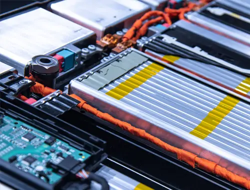
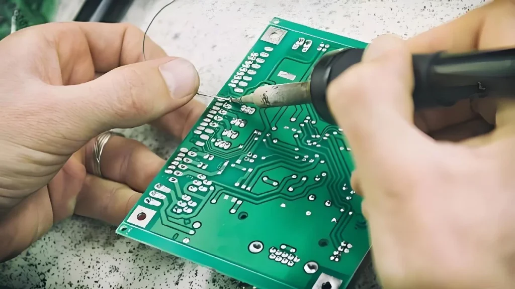
FPC surface treatment is not merely an optional auxiliary process, but a critical step that determines soldering reliability and storage life. Bare copper is highly susceptible to oxidation; without protection, subsequent processes such as surface-mount assembly and bonding face a high risk of failure. Different surface treatment processes correspond to varying costs, performance characteristics and suitable applications; understanding their fundamental nature is the foundation for ensuring FPC quality.
Why FPC Surface Treatment Has Become a Critical Stage in PCB Manufacturing
The core objective of FPC surface treatment is essentially to address the inherent flaw of bare copper when exposed to air—copper foil oxidises very easily, and the resulting oxide layer can directly lead to soldering failures, increased contact resistance, and even circuit short-circuits, rendering the entire FPC inoperable. In addition, a high-quality surface treatment process must fulfil three key functions, which are the primary reasons why it has become an indispensable stage in PCB manufacturing.
1.Protecting the copper surface by isolating it from corrosive agents such as air and moisture, thereby extending the storage life and service life of the FPC.
Bare copper forms an oxide layer within a few hours at room temperature; however, following surface treatment, the storage life of the FPC can be extended to over six months, with some high-end processes achieving over a year, significantly reducing warehousing and wastage costs.
2.Ensuring good solderability and electrical conductivity
Providing a stable interface for subsequent processes such as SMT placement, bonding and insertion/removal, thereby reducing production defects such as cold solder joints and false solder joints, and improving the yield rate of PCB manufacturing.
3.Meeting Application Requirements
Surface treatment requirements for FPCs vary greatly across different sectors. For example, FPCs for wearable devices must balance flexibility with abrasion resistance; those for 5G equipment must ensure the stability of high-frequency signal transmission; whilst FPCs for medical devices have extremely high corrosion resistance requirements.
Common FPC Surface Treatment Processes
Electroless nickel-gold (ENIG, commonly known as electroless gold plating) is currently the most widely used surface treatment process for FPCs, and is an ‘all-round’ option that balances performance and practicality. The principle involves using a chemical reaction to first deposit a layer of nickel onto the copper foil surface as a barrier layer, followed by a thin layer of gold as a protective layer. The nickel layer prevents diffusion between the gold and copper, whilst the gold layer provides oxidation resistance and enhances conductivity.
The core advantages of this process include a smooth surface finish, suitability for fine-pitch pads and bonding processes, excellent solderability, a long storage life, and minimal impact on the flexibility of the FPC. It is suitable for almost all mid-to-high-end FPC products, and is particularly well-suited to applications with high reliability requirements, such as mobile phone camera modules and medical devices.
However, its shortcomings are also quite evident: the cost is higher than that of OSP and electroless tin plating processes, and there is a risk of ‘black pads’; if the phosphorus content in the nickel layer is not properly controlled, it may lead to a reduction in solder joint strength.
Electrolytic hard gold plating, on the other hand, is a targeted process focused on ‘wear resistance and resistance to repeated mating and unmating’. Unlike the chemical deposition used in electroless gold plating, it involves electroplating a hard gold layer containing elements such as cobalt and nickel onto the surface of the copper foil. The thickness of this gold layer is significantly greater than that of electroless gold plating,typically ranging from 0.1 to 0.3 μm, and can be increased to 0.5 μm in certain high-end applications.
Its greatest advantage lies in its exceptional wear resistance and stable contact resistance, making it suitable for connector gold fingers, test points and other areas requiring frequent insertion and removal, such as interfaces in wearable devices and FPC connectors in automotive electronics. However, this process is the most expensive and complex, and the thick gold layer may affect the flexibility of the FPC;consequently,it is typically used for localised treatment rather than full-board treatment.
OSP (Organic Solderable Protective Coating) is the most cost-effective and environmentally friendly surface treatment process. It works by applying a thin film of organic nitrogen compounds to a clean, bare copper surface, forming a dense protective layer that prevents the copper foil from oxidising. Its advantages are significant: the process is simple and highly efficient, the surface is smooth, it does not affect the flexibility of the FPC, and it complies with RoHS environmental standards.
It is suitable for simple FPC products that are cost-sensitive, have low circuit density, and require rapid soldering, such as low-end sensors and remote control flexible circuits. However, its shortcomings are also quite evident: the protective film is fragile and prone to scratching, it does not withstand multiple reflow soldering cycles, it has a short shelf life (typically 3–6 months), and it is unsuitable for contact areas requiring frequent plugging and unplugging.
Both silver plating and tin plating processes are cost-effective options for the mid-to-low end of the market. Their core advantages lie in good solderability, moderate cost, and a smooth surface, making them suitable for fine-pitch pads. The silver plating process deposits a thin layer of silver onto the copper foil surface via a chemical displacement reaction. It offers excellent conductivity and is particularly suitable for high-frequency signal transmission applications such as 5G antennas.
However, the silver layer is prone to oxidation and sulphidation, requiring vacuum-sealed storage, and there is a risk of silver migration, which can affect insulation performance. The tin plating process, on the other hand, uses chemical displacement to deposit a layer of pure tin. It offers good compatibility with lead-free solder, is environmentally friendly and costs less than silver plating.
However, the tin layer is relatively soft and prone to scratching, carries a risk of tin whisker growth, and its performance tends to deteriorate in high-temperature environments. It is suitable for consumer electronics products with modest requirements regarding storage and operating conditions.
Electrolytic Nickel-Palladium-Gold (ENEPIG) is the ‘top-of-the-range’ process for high-end applications. It incorporates a palladium layer between the nickel and gold layers; this palladium layer effectively prevents displacement reactions between the nickel and gold, thereby enhancing protective performance and soldering reliability. Its advantages include exceptional corrosion resistance, making it suitable for extreme environments such as military and aerospace applications.
It is compatible with various soldering methods and offers high surface flatness, making it ideal for high-end FPC products requiring ultra-fine pitch and high reliability.However, this process is extremely costly, complex, and demands strict control over production environments and parameters; consequently, it is currently limited to a few high-end sectors and has not yet become widespread.
It is worth noting that although the lead-free hot air solder levelling (HASL) process is widely used in rigid PCBs, the high temperatures involved (240–270°C) can cause severe damage to the PI substrate of FPCs, leading to delamination, embrittlement and fracture under bending.Consequently, it has been largely phased out of mainstream FPC manufacturing and is now used with caution only in a very small number of low-end, simple flexible circuits.
As the FPC industry evolves towards ultra-thin, high-density and eco-friendly designs, surface treatment processes are also undergoing continuous iteration. New technologies, such as cyanide-free electroplating and the application of self-healing polyimide materials, are addressing the shortcomings of traditional processes; simultaneously, the industry’s demands for process precision are constantly rising.
The integration of precision processes such as laser direct imaging (LDI) has significantly improved the uniformity and consistency of plating layers.For PCB manufacturers, only by delving deeply into the finer details of the process and exercising precise control over material selection and quality can they gain a competitive edge in the FPC market.
FPC surface treatment processes may appear to be a ‘supporting stage’ in PCB manufacturing, but in reality, they are the core factor determining product reliability and competitiveness.From ordinary consumer electronics to high-end military equipment, and from 5G communications to wearable devices, every high-quality FPC relies on appropriate surface treatment processes for its performance.
Only by understanding the characteristics and suitable applications of each process, and implementing comprehensive quality control throughout the entire process, can we unlock the secret to FPC reliability and drive the PCB manufacturing industry towards steady development in the direction of high-end and precision manufacturing.
No single surface treatment process is suitable for all scenarios; the key lies in selecting the appropriate process based on the product’s actual requirements and strictly controlling the process window.From ENIG to ENEPIG, and from OSP to electroless silver plating, each process has its own advantages and limitations. Only by mastering surface treatment can the true reliability of FPCs be realised.