HDI PCB(High Density Interconnect) is a core PCB manufacturing process designed for high-density wiring, characterised primarily by the use of micro-blind vias and buried blind vias to achieve efficient interconnection between different copper layers within the circuit board. As electronic products rapidly evolve towards lighter, thinner and higher-performance designs, market demand for HDI boards continues to grow.
Definition and Classification of HDI
HDI PCB, formally known as high-density interconnect multilayer boards, constitute a significant category within rigid printed circuit boards. Unlike traditional through-hole multilayer boards, which rely on through-holes penetrating the entire board thickness, the core feature of HDI boards lies in connecting specific layers solely via micro-blind vias and buried blind vias.
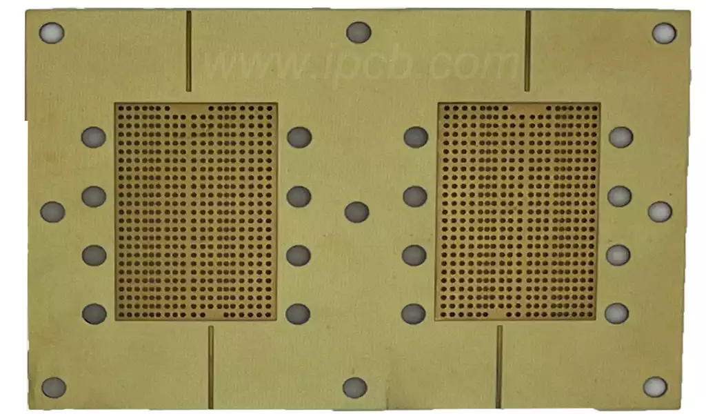
Broadly speaking, any HDI PCB utilising micro-blind or buried blind vias may be termed an HDI board. These micro-blind and buried blind vias are typically created through a layer-stacking process and can be classified as first-order, second-order, third-order, or Anylayer HDI based on the number of layers; of these, Anylayer represents the highest density type within the process.
The source of HDI PCB’s high-density characteristics
The high-density routing capability of hdi pcb stems primarily from two factors:
Space-saving blind/buried vias: In standard multilayer boards, through-holes penetrate the entire board, occupying a significant amount of space that could otherwise be used for routing; whereas blind vias and buried blind vias connect only the required layers, thereby freeing up a substantial amount of routing space and increasing routing density.
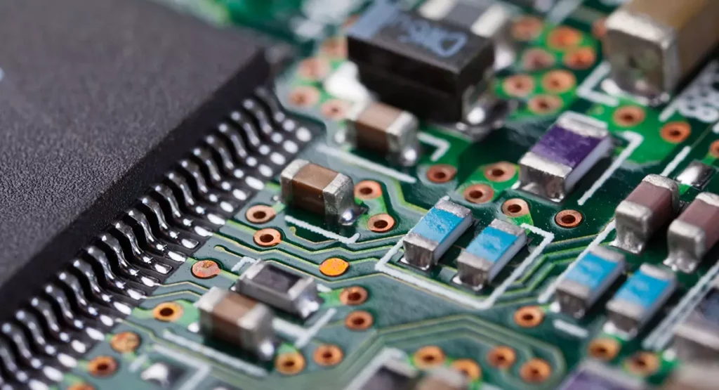
Micro-holes achieved through laser drilling: Blind and buried-blind vias are predominantly created using laser drilling technology (which burns through the resin dielectric layer to form the hole). Compared to mechanical drilling, laser drilling can achieve much smaller hole diameters. To achieve the same level of fineness with mechanical drilling, the drill bit is highly prone to breakage and the cost is prohibitively high.
Generally speaking, the greater the number of blind and buried vias, the higher the routing density of the HDI board; that is, as the HDI tier increases, so does the density. As the highest-tier HDI, Anylayer has reached the limit of density. To further increase density, the industry has introduced modified semi-additive processes (mSAP) and substrate technologies based on HDI, resulting in the production of substrate-like panels (SLP). It is thus evident that HDI serves as a crucial foundation for achieving high-density routing.
Main Application Areas
The application of HDI PCB has gradually expanded from the initial high-tech sectors such as aerospace and defence to civilian and industrial scenarios including consumer electronics, telecommunications equipment and automotive electronics. Their core advantages include: smaller dimensions, higher component integration density, superior signal integrity and enhanced electrical performance. They are particularly suitable for lightweight, slim, compact electronic products such as smartphones, tablets and wearable devices, as well as high-performance computing and data centre equipment.
It is worth noting that high-speed communication products, such as those for AI, have traditionally relied primarily on high-layer-count boards (communication equipment typically uses 8–16 layers, whilst server and storage equipment mainly uses 6 layers or 8–16 layers). With increasing bandwidth and chip upgrades, HDI boards have successfully transitioned from the consumer electronics sector into the high-speed communications sector by meeting the stringent requirements of high-speed signal transmission.
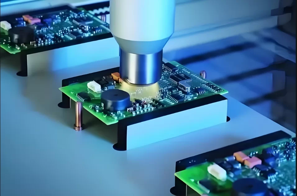
Production Process
The production process for HDI PCB is complex and intricate, with the main stages including:
Preparation of raw materials: nickel-copper foil, multilayer laminates, prepregs, etc.;
Circuit Design and Fabrication: Design of inner and outer layer circuit patterns, followed by copper plating, photolithography, film removal and etching to form the circuit;
Multilayer Board Lamination: Assembling multiple layers of circuit boards according to the design specifications to achieve interlayer connectivity;
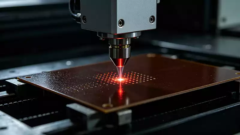
Laser Drilling: Using lasers to drill micro-blind and buried blind vias to meet the requirements for thinner and lighter designs;
Electroplating and lamination: Electroplating forms conductive paths, whilst lamination ensures structural stability;
Laser via plugging: Creating microscopic air holes on the HDI PCB board surface to eliminate internal stress and enhance thermal resistance and mechanical strength;
Other auxiliary processes: Cutting, inner layer dry film, blackening/browning, electroless copper plating and copper thickening, second inner layer dry film, etc.
Key Growth Drivers
1.AI Servers: High integration and complex interconnects are driving a surge in demand for HDI PCB
HDI boards are the fastest-growing segment within the server PCB market. According to Prismark data, the global PCB market for servers and related system components was valued at approximately US$5.177 billion in 2023 and is projected to grow to US$7.974 billion by 2028 (a compound annual growth rate of 9%).
The three core products of AI servers—GPU motherboards, OAM accelerator cards and network interface cards—are all expected to adopt HDI solutions across the board in the future. Prismark forecasts that the compound annual growth rate (CAGR) for HDI boards between 2023 and 2028 will reach 16.3%, ranking first among all PCB categories.
AI servers impose stringent requirements on high-frequency, high-speed signal transmission, high chip integration, complex interconnect structures and efficient thermal management, driving a continuous increase in the demand for high-end HDI. Taking NVIDIA’s AI computing chips as an example, from the A100 and H100 to the B100 and GB200, there have been leapfrog improvements in chip area, interconnect methods, bandwidth and memory capacity.
The GB200 boasts 30 times the computing power of the H100, with memory and bandwidth significantly surpassing its predecessor, placing higher demands on PCB specifications and accelerating the adoption of high-end HDI.
High-frequency, high-speed transmission: The GB200 NVL72 utilises NVLink full-connectivity technology, offering a bidirectional bandwidth of up to 900 GB/s, necessitating the use of M7-grade or higher PCB materials to minimise crosstalk and ensure signal integrity.
Complex Interconnect Structures: The GB200 NVL72 utilises backplane connectors and OverPass jumper cables to address crosstalk issues. With NVLink 5.0 technology offering a bandwidth of 1,800 Gbps, it is particularly well-suited to HDI PCB with high signal rates. Complex structures such as NVLink switch module boards demand extremely high levels of design precision and reliability, which align perfectly with the microvia and high-density characteristics of HDI.
High Integration and Thermal Management: The GB200 chip comprises two B200 GPUs (each with approximately 208 billion transistors) and a Grace CPU. Utilising liquid cooling technology, it requires HDI PCBs with highly efficient thermal management capabilities and high-temperature stability. HDI pcbs offer significant advantages in terms of functional integration and space utilisation, enabling increased routing density and optimised thermal management to meet AI server specifications.
Taking the NVIDIA GB200 NVL72 system as an example, high-end AI servers have seen a substantial increase in the use of high-tier HDI. This system comprises 18 compute trays and 9 switching trays: each compute tray contains two GB200 superchips, accompanied by 2 motherboards, 1 backplane, 4 network interface cards, and 1 DPU board, all utilising high-tier HDI solutions; each NVLink switching tray contains 1 NVLink switch module board, employing high-layer or HDI solutions.
2.Automotive Electronics: Intelligent Upgrades Drive Growth in Both HDI Specifications and Volume
HDI PCBs offer advantages such as miniaturisation, high density and superior signal transmission, making them suitable for core components including autonomous driving systems, driver assistance equipment, in-vehicle radar and in-car entertainment systems. As the electrification and intelligentisation of vehicles continue to advance, the market share of HDI pcbs, FPCs and high-frequency boards is gradually increasing.
Intelligent driving systems (particularly LiDAR) impose extremely high demands on resolution, interference resistance and size control, making them a core application scenario for HDI boards; in-vehicle cameras predominantly utilise rigid boards or rigid-flex boards. Concurrently, the increasing level of automotive intelligence is driving the transition of HDI pcbs from 2-layer and 3-layer to 4-layer and beyond, to meet the interconnection requirements of complex sensors and controllers.
Thanks to its high-density routing, excellent signal integrity and suitability for thin, lightweight, high-performance designs, HDI technology has become an indispensable foundational process in modern electronic systems. In the future, with the deepening development of 5G/6G communications, edge computing and autonomous driving, HDI pcbs will evolve further towards higher density, improved heat dissipation and more reliable interconnections, and are expected to become one of the most sustainably growing and dynamically innovative segments within the PCB industry.