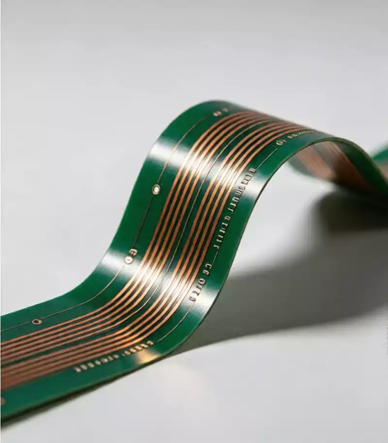
Flexible printed circuit boards (FPCs), with their inherent properties of being bendable, foldable, lightweight, and compact, are ideally suited to the requirements of tight spaces and complex structural assemblies in sectors such as smartphones, wearable devices, automotive electronics, medical instruments and aerospace. They have become an indispensable core interconnect component in modern electronic products.
The Core Value and Underlying Logic of FPC Laminate Design
FPC laminate design is a systematic process involving the hierarchical arrangement, thickness ratio and structural symmetry of functional materials such as the substrate, conductive layers, adhesive layers, cover layers and reinforcement layers; it is by no means a simple stacking of materials.Its core objective is to achieve three key balances:
The balance between flexibility and strength
The balance between electrical performance and mechanical performance
The balance between reliability and cost
From a mechanical perspective, FPCs generate complex internal stress distributions during bending, torsion and vibration. The laminate structure directly determines the stress concentration points, the position of the neutral axis and the minimum bending radius—asymmetrical laminates are prone to causing curling, delamination and conductor fatigue failure, whereas a rational laminate design can distribute stress evenly, extending the bending life to over a million cycles.
From an electrical performance perspective, the laminate design directly influences impedance control, signal transmission, electromagnetic compatibility (EMC) and heat dissipation efficiency. In high-frequency, high-speed applications, the selection of dielectric materials and the design of layer spacing are particularly critical to signal integrity.
From a manufacturing perspective, a scientifically sound laminate scheme can accommodate the requirements of processes such as etching, lamination, drilling and electroplating, thereby reducing production defect rates and enhancing the stability of mass production.
It can be said that FPC laminate design lies at the intersection of materials science, structural mechanics, electronic engineering and manufacturing processes. It serves as the first line of defence in ensuring that FPCs progress from design drawings to reliable products, and is a key technological factor enabling high-end electronic products to achieve competitive differentiation.
Key Considerations for FPC Laminate Design
1.Selection of Base Materials
The materials determine the FPC’s flexibility, temperature resistance, dielectric properties and mechanical strength, and must be precisely matched to the specific application.
Insulating Substrates
Polyimide (PI): The industry standard, with a temperature resistance exceeding 250°C, excellent flexibility and strong chemical stability; suitable for high-end applications such as automotive, medical and aerospace sectors.
Polyester (PET): Lower cost, temperature resistance of approximately 105°C, suitable for static bending applications in consumer electronics.
Liquid Crystal Polymer (LCP): Low dielectric loss and low moisture absorption, making it the preferred choice for high-frequency, high-speed applications such as 5G and millimetre-wave radar.
Common substrate thicknesses are 12.5μm, 25μm and 50μm; the thinner the substrate, the better the flexibility, but processing difficulty increases accordingly.
Conductive Copper Foil
Rolled Anodised (RA): Elongation >15%, dense molecular structure, resistant to repeated bending; the essential material for dynamic bending applications (e.g. foldable screens, robotic joints).
Electrolytic Copper (ED): Lower cost, suitable for static, single-use bending applications.
Common copper foil thicknesses are 1/2 oz (18 μm) and 1 oz (35 μm); thinner copper foil is preferred for dynamic bending to minimise bending stress.
Adhesive Layer
Acrylic Adhesive: Low cost and stable adhesion, the preferred choice for standard FPCs.
Adhesive-free substrate: The adhesive layer is removed through direct lamination, resulting in thinner thickness, better temperature resistance and lower signal loss; suitable for high-frequency and high-reliability applications.
Covering Layer
PI cover film: Highly flexible, used to replace traditional solder mask layers to protect circuits; thickness 12.5–25 μm.
Photosensitive solder mask ink: High precision, suitable for fine circuits, but with slightly lower flexibility; not recommended for bending areas.
Reinforcement materials
Commonly used materials include FR4, PI and stainless steel, employed in areas requiring support such as connectors and soldering zones to enhance local stiffness and prevent breakage during insertion, removal or soldering.
2.Neutral Axis Control
The neutral axis is the central plane of an FPC that is subject to neither tension nor compression when the FPC is bent. Positioning the conductor layers near the neutral axis minimises bending stress—this is a core principle of FPC stack-up design.
Symmetrical Stack-up: Dual-layer and multi-layer FPCs should adopt a top-to-bottom symmetrical structure. For example, in a double-sided FPC, the copper foils on both sides should be of equal thickness, and the substrate and cover layers should be symmetrical. This ensures the neutral axis is centred, preventing board warping and stress displacement.
Optimisation of multi-layer FPCs: Concentrating conductor layers near the neutral axis reduces the number of conductors in high-stress areas, thereby lowering the risk of fracture during bending.
Asymmetry compensation: Where complete symmetry cannot be achieved due to functional requirements, stress deviations can be compensated for by adjusting material thickness or the number of layers, thereby minimising neutral axis displacement as much as possible.
3.Bending Performance Matching
Depending on the bending conditions, FPCs can be categorised into static bending (bend once during assembly, with no further movement throughout the service life), dynamic bending (repeated bending during use), and high-flex torsion (robots, wearable devices). The laminate design must be tailored accordingly:
Minimum bending radius: ≥6 times the board thickness for static bending, ≥10 times the board thickness for dynamic bending; for multilayer boards, the radius should be further increased to prevent copper foil fatigue fracture.
Bending Zone Restrictions: Via holes, pads, components and right-angled traces must not be placed within the bending radius to avoid cracking caused by stress concentration; traces should run perpendicular to the bending direction and be evenly distributed to reduce localised stress.
Dynamic Bending Reinforcement: Select ultra-thin rolled copper, adhesive-free substrates and thin PI to reduce the total stack thickness and improve bending life.
4.Electrical Performance Requirements
Impedance Control: High-frequency and high-speed signals require precise control of single-ended impedance (e.g. 50Ω) or differential impedance (90Ω/100Ω). This is achieved by adjusting the thickness of dielectric layers, trace width, trace spacing and copper foil thickness. When designing the stack-up, sufficient margin must be allowed for impedance simulation to avoid interlayer interference.
Electromagnetic Shielding: Multi-layer FPCs should incorporate ground planes and shielding layers, arranged in an ‘adjoining signal-ground’ configuration to suppress electromagnetic interference; in high-frequency applications, low-Dk/Df materials should be selected to minimise signal loss.
Current-Carrying Capacity: In high-current applications, copper foil thickness must be increased and ground plane design optimised to enhance heat dissipation and current-carrying capacity, thereby preventing circuit overheating.
5.Planning the Number of Layers
FPCs range from single-layer to eight layers or more. The greater the number of layers, the higher the integration density; however, this results in reduced flexibility, increased costs and greater manufacturing complexity.
Single-layer FPC: Simple structure with excellent flexibility, suitable for simple signal transmission in printers, consumer electronics connectors, etc.
Double-layer FPC: Double-sided routing with improved integration; the symmetrical structure ensures the neutral axis remains centred, making it the most widely used type.
Multi-layer FPC (4–8 layers): Suitable for high-density routing; requires strict control of total thickness and the use of symmetrical stacking, commonly used in mobile phones and automotive electronics.
Rigid-flex boards: The rigid section (FR4) supports components, whilst the flexible section enables bending, balancing structural support with flexibility. The laminate design must focus on the transition structure between rigid and flexible zones to avoid sudden changes in stress.
6.Process and Cost Alignment
Laminate design must align with the factory’s process capabilities to avoid cost escalation caused by over-engineering.
Process Compatibility: Ensure parameters such as layer spacing and thickness ratios comply with process standards for lamination, etching, laser drilling and electroplating.
Cost Control: Whilst meeting performance requirements, prioritise standard materials and thicknesses, minimise the number of layers and specialised processes, and balance cost-effectiveness.
Reliability Validation: The laminate design must pass validation tests including bending, high and low temperature cycling, and humidity-heat ageing, and comply with industry standards such as IPC-2223 and IPC-6013 and other industry standards.
Industry Best Practices for FPC Lamination Design
1.Classic Lamination Structures
Single-layer FPC: Top PI cover film + adhesive layer + copper foil + PI substrate + adhesive layer + bottom PI cover film, total thickness approx. 140μm, suitable for static, simple routing.
Double-layer symmetrical FPC: Top and bottom PI cover films + adhesive layer + equal-thickness rolled copper + PI substrate, with a total thickness of approximately 160 μm. The neutral axis is centred, offering excellent dynamic bending performance.
Multi-layer high-frequency FPC: Utilises an adhesive-free LCP substrate with alternating signal and ground layers, offering low dielectric loss and suitability for high-frequency applications such as 5G and millimetre-wave.
Rigid-flex boards: The rigid section features a multi-layer FR4 structure, the flexible section an ultra-thin adhesive-free PI structure, and the transition zone employs a gradient window design to prevent stress concentration.
2.Key Design Specifications
Prioritise symmetry: FPCs with two or more layers must employ a symmetrical stack-up to ensure symmetrical thicknesses of conductor layers, base materials and cover layers, thereby guaranteeing the neutral axis is centred.
Minimalist design in bending zones: Retain only essential traces in bending areas, avoiding vias, pads and copper fills; route traces perpendicular to the bending direction and use curved transitions.
Precise Reinforcement: Reinforcement should only be added to stress-bearing areas such as connectors and soldering zones; edges should be chamfered to reduce stress concentration.
High-Frequency Signal Optimisation: High-frequency layers should be kept away from power layers; signal paths should be shortened; a continuous ground plane should be used to avoid segmentation.
Simulation-Led Validation: Stress and impedance simulations should be performed using software such as ANSYS to optimise the stack-up scheme in advance, thereby reducing trial-and-error costs.
3.Key Points for Failure Prevention
Eliminate curling and delamination issues caused by asymmetrical stacking.
Electrolytic copper must not be used in areas subject to dynamic bending to prevent conductor fatigue failure.
Strictly adhere to minimum bending radius standards in bending areas—approximately 78% of FPC failures stem from non-compliance with bending radius requirements.
For multi-layer boards, control the total thickness to prevent loss of flexibility due to excessive thickness.
Select materials with matched CTE for high- and low-temperature applications to minimise delamination caused by thermal expansion and contraction.
Trends in FPC Laminate Design
As electronic products evolve towards foldable, miniaturised, high-frequency and automotive-grade specifications, FPC laminate design is exhibiting three major trends:
Ultra-thin: Adhesive-free substrates and ultra-thin PI/copper foil are becoming increasingly widespread, with total laminate thicknesses capable of being reduced to below 50μm.
High-frequency and high-speed performance: The large-scale application of low-loss materials such as LCP and MPI is driving laminate design towards precise impedance control and integrated shielding.
High reliability: Automotive-grade and medical-grade FPC laminates place greater emphasis on symmetrical design and stress optimisation to meet requirements for millions of bending cycles and harsh environmental conditions.
Integration: Laminate solutions for rigid-flex boards and embedded components are maturing, further enhancing space utilisation and system integration.
FPC laminate design is by no means a simple layering of materials, but rather a precise collaboration spanning materials science, structural mechanics and electronic engineering. Looking towards a future characterised by foldability, high-frequency operation and high reliability, layup design will remain the pivotal factor determining the success or failure of FPC products.