The stack up design of a PCB (printed circuit board) directly determines its electrical performance, mechanical reliability, manufacturability and cost. Among these, Through Hole Board and HDI boards are the two main types, and there is a fundamental difference in the underlying logic of their stack up designs—this difference stems from the fundamental differences between the two in terms of via types and lamination processes, which in turn manifests as distinctions in structural complexity, performance and applicable scenarios.
Through Hole Board
The stack up design of Through Hole Board is consistently centred on ‘mature processes, optimal cost, and meeting standard electrical requirements’. Their core characteristic is the reliance on through-holes (PTH) that penetrate the entire board to achieve interlayer interconnection. The structure is simple, requiring no complex interlayer connections, and is suitable for standard electronic equipment operating at medium to low speeds that does not require miniaturisation.
1.Stacking Characteristics
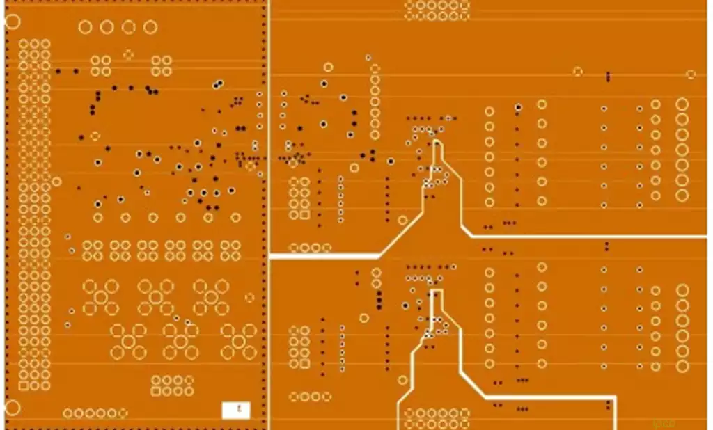
Exclusive use of through-holes (PTH): Via holes pass directly from the top copper foil to the bottom copper foil, traversing the entire substrate. The hole walls are electroplated to ensure electrical continuity between layers, eliminating the need for laser drilling or layered interconnection processes.
High space consumption: Through-holes occupy a significant amount of space on both outer and inner layers, limiting routing density and precluding high-density interconnection.
Simple structure: There is no complex interlayer nesting, making the design simple and reliable.
2.Common stack up types (using a 4-layer board as an example)
Through Hole Board follow the basic logic of ‘signal-power-ground’, with common layer counts being 2, 4, and 6 layers. Among these, the 4-layer board is the most common specification in the industrial and consumer electronics sectors, with a typical stack up as follows:
Top signal layer → Inner ground layer → Inner power layer → Bottom signal layer
This structure achieves separation of signals from power and ground: the inner power and ground layers not only provide stable power and a reference ground for the top and bottom signal layers, but also effectively shield against signal interference and reduce EMI radiation, meeting the transmission requirements of medium-to-low-speed signals such as serial ports and general I/O.
For 2-layer Through Hole Board, the structure is simpler, consisting solely of a ‘top signal layer – bottom signal layer’; power and ground must be routed via surface-level traces, making them suitable for devices with lower electrical performance requirements, such as toys and simple controllers.
3.Key Advantages
Low manufacturing barriers: No complex processes such as laser drilling or sequential lamination are required; standard PCB manufacturers can produce them.
Controllable costs: Through-hole processing and lamination processes are straightforward, and standard FR-4 material is sufficient to meet requirements. Compared to HDI boards, costs can be reduced by 30% to 60%.
High reliability: Through-holes offer strong electrical continuity and are less prone to interlayer disconnections or poor contact, making them suitable for cost-sensitive applications with moderate performance requirements, such as industrial control, household appliances and general consumer electronics.
HDI Boards
The stack up design of HDI boards is centred on ‘overcoming spatial constraints and enhancing signal performance’. It utilises laser-drilled micro-blind vias and buried vias in place of traditional through-holes, combined with a sequential lamination process, to achieve high-density interconnections between layers, thereby resolving the routing challenges associated with miniaturised, high-speed products. Unlike Through Hole Board, which involve “single-pass lamination with through-holes across the entire board”, the stack up of HDI boards is more complex. However, this enables them to meet the stringent size and performance requirements of products such as smartphones, tablets, automotive chips and high-end medical equipment.
1.Structural Characteristics
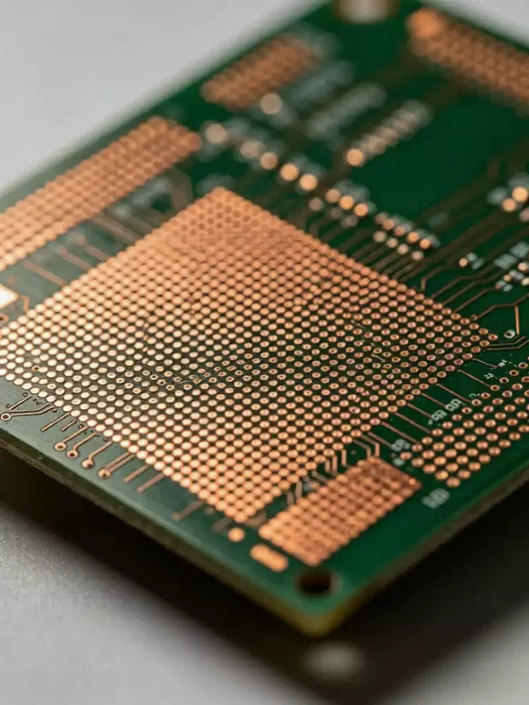
Laser-drilled micro-blind vias + sequential lamination: Micro-blind vias typically have a diameter of 0.1–0.2 mm (significantly smaller than the 0.2–0.3 mm of through-holes). Blind vias interconnect outer layers with inner layers, whilst buried vias interconnect inner layers, thereby avoiding the space wastage caused by through-holes penetrating the entire board. The sequential lamination process (first manufacturing the core board, then sequentially adding and laminating additional layers) enables precise control over the thickness of the dielectric and copper layers, ensuring the reliability of the interconnections formed by micro-blind and buried vias.
High routing flexibility: Through multi-layer stacking and the use of micro-blind vias, PCB dimensions can be significantly reduced—for the same functionality, the area of an HDI board can be 40%–60% smaller than that of a through-hole board, which is key to its role as the core carrier for miniaturised products.
2.Common stack up types (classified by the number of laser-drilled blind via levels)
HDI board stack ups are categorised into 1-layer, 2-layer and Anylayer types. The higher the level, the more complex the structure, the greater the routing flexibility, and the cost increases exponentially.
1-Stage (1-N-1): The most cost-effective entry-level HDI. This involves first manufacturing a 4-layer through-hole core board, then adding one signal layer each to the top and bottom surfaces of the core board. Interconnection between the added layers and the core board is achieved via laser-drilled micro-blind vias, whilst retaining some mechanical through-holes for auxiliary interconnection. For example, a 6-layer 1st-order HDI board is effectively a ‘4-layer through-hole core board + top signal layer + bottom signal layer’, suitable for mid-to-low-end smartphones, smart wearable devices and other products with specific size requirements but cost-sensitive constraints.
2nd-order (2-N-2): This adds a layer of laser-drilled blind vias to the 1st-order structure, forming a two-layer laser-drilled blind via configuration, which is divided into two processes: offset vias and stacked vias. In the staggered-hole process, the two layers of blind vias are arranged in an offset configuration, eliminating the need for fill-and-plating, resulting in lower costs but slightly reduced space utilisation for routing.
In the stacked-hole process, the two layers of blind vias are stacked vertically, requiring the lower-layer blind vias to be filled and plated before drilling the upper-layer blind vias. This process is more complex and costly, but maximises space efficiency. 2nd-order HDI is suitable for products with densely packed core chip pins and complex routing requirements, such as high-end smartphones, tablets and in-vehicle infotainment systems.
Anylayer: The highest-order HDI, where all layers utilise stacked laser-drilled blind/buried vias, eliminating the need for mechanical through-holes. Any two layers can be interconnected via micro-blind vias, offering exceptional routing flexibility. It can accommodate high-end chips with a pin pitch of ≤0.3mm (such as CPUs and GPUs), but the manufacturing process is extremely challenging. It requires the use of special materials such as RCC (resin-coated copper foil), making it costly and suitable only for high-end military, medical, and server applications where performance demands are extreme.
Comparison of stack up Designs for Through Hole Board and HDI Boards
1.Electrical Performance: Through Hole Board meet standard requirements, whilst HDI boards strive for excellence
Both require attention to impedance control and signal integrity, but the requirements differ significantly.
Impedance Control: Both require strict control of dielectric thickness, trace width and material dielectric constant (Dk) to ensure common impedances such as 50Ω and 75Ω, with deviations typically kept within ±10%. However, due to their higher routing density, finer trace widths (0.08–0.12 mm, compared to 0.15–0.2 mm for Through Hole Board) and thinner dielectric thickness (0.1–0.2 mm, compared to 0.2–0.4 mm for Through Hole Board), HDI boards demand greater precision in impedance control. Materials with stable dielectric constants (such as high-speed materials or RCC) must be selected.
Signal integrity: High-speed signals (such as DDR4, DDR5, USB 3.0 and above) should be routed on inner layers adjacent to ground planes, forming microstrip or stripline structures to reduce EMI and crosstalk. Through Hole Board have fewer high-speed signal requirements, so simple ground shielding is sufficient; whereas HDI boards are frequently used in high-speed products, with greater emphasis placed on ground plane layout within the stack up. An alternating ‘signal layer–ground layer’ structure is commonly adopted to ensure stable high-speed signal transmission.
2.Manufacturability and Cost: Through Hole Board offer outstanding value for money, whilst the cost of HDI boards increases with the number of layers
Principle of Laminating Symmetry (Common Requirement): The stack up of both types of PCBs must maintain complete symmetry—symmetrical copper thickness, symmetrical dielectric thickness, and balanced copper residue.
Otherwise, differing shrinkage rates between layers during high-temperature lamination will generate internal stress, leading to board warping, which affects SMT placement accuracy and may even result in cold solder joints or chip damage. In the automotive and defence sectors, board warpage and camber tolerances are typically required to be ≤0.7%, which is a strict threshold.
Vehicle Diameter and Process Costs: Through Hole Board commonly use 0.2–0.3 mm drill bits. Whilst 0.2 mm through-holes incur slightly higher costs than 0.3 mm due to slower drilling speeds and a higher risk of drill breakage, the overall process cost remains lower. The cost of HDI boards primarily depends on the number of layers and the manufacturing process: 1-layer HDI costs only 20%–30% more than a through-hole board with the same number of layers.
2-layer HDI costs 1.5–2 times that of a through-hole board with the same number of layers; and any-layer HDI can cost 3–5 times that of a through-hole board with the same number of layers. Furthermore, the stacked via process costs over 30% more than the staggered via process. Laser drilling and fill-level plating further increase manufacturing costs.
3.Space and Layout: Through Hole Board offer greater flexibility, whilst HDI boards overcome limitations
BGA pitch adaptation: The centre-to-centre distance of BGA (Ball Grid Array) chip pins directly determines the choice of stack up. If the pin pitch is >0.5 mm, there is sufficient routing space on a through-hole board to achieve fan-out via conventional through-holes; if the pin pitch is ≤0.4 mm, the through-holes on a through-hole board occupy too much space to allow fan-out, necessitating the use of micro-blind vias on an HDI board—this is the core reason why high-density BGA chip products such as smartphones and tablets must adopt HDI.
Differences in routing density: Conventional industrial and consumer electronics (such as household appliances and standard controllers) can meet requirements using 4–6-layer Through Hole Board; whereas smart products (such as smartphones and smartwatches) generally employ 8-layer Class 1 to 10-layer Class 2 HDI designs, with some high-end models even utilising 12-layer Class 2 or arbitrary-layer HDI to achieve the ultimate in miniaturisation.
4.Thermal Management and Material Selection: Adapting to Different Application Environments
Thermal Management: Due to their high routing density and dense microvia arrangement, HDI boards offer a larger heat dissipation area, which aids heat dissipation; however, it should be noted that fine traces (≤0.1 mm) have a relatively low current-carrying capacity, and excessive current can easily lead to overheating or burnout. Therefore, the width of power traces and copper thickness must be carefully planned within the HDI board stack up. Through Hole Board feature wider traces and higher current-carrying capacity, resulting in lower thermal management demands; the primary concern is to avoid uneven heat dissipation caused by large areas of concentrated copper.
Material Selection: Through Hole Board typically utilise standard FR-4 (Dk ≈ 4.4), which offers low cost and stable performance, suitable for low to medium-speed, ambient-temperature environments. If HDI boards are to be used in high-speed, high-temperature environments (such as automotive or server applications), high-speed materials (e.g. PTFE, Dk ≈ 2.6–3.0) or RCC must be selected. These materials offer stable dielectric constants, high-temperature resistance and good heat dissipation, but come at a higher cost; for standard mid-to-low-end HDI products, modified FR-4 can be used to balance cost and performance.
The design of through-hole and HDI board stack ups essentially involves a trade-off between ‘cost efficiency’ and ‘spatial performance’. Through Hole Board dominate conventional electronic devices due to their simplicity, reliability and low cost; HDI boards, on the other hand, have become the inevitable choice for high-density, high-speed products thanks to micro-blind vias, sequential lamination and high-order interconnects. Understanding the underlying logic and key differences between the two is fundamental to the rational selection and efficient design of PCBs.