Unlike standard PCBs, the core of multilayer RF PCB design lies in balancing signal integrity with manufacturability. High-frequency signals are prone to attenuation, reflection and crosstalk during transmission, and the complexity of multi-layer structures further exacerbates these issues.
The core value of multilayer RF PCBs lies in utilising three-dimensional routing to overcome the performance limitations of planar boards, enabling high-density routing within a limited space whilst suppressing electromagnetic interference through scientific layer stacking. Compared to standard multilayer PCBs, the design differences primarily centre on signal adaptation, material selection and layer stacking planning; these three aspects are also the areas most prone to issues in day-to-day design.
Material selection forms the foundation of multilayer RF PCB design, directly determining signal transmission efficiency and environmental adaptability. Many novice engineers fall into the misconception that ‘the more high-end the material, the better’; in reality, the logic behind material selection varies significantly across different scenarios, and blindly opting for high-end materials will only result in wasted costs.
The stability of the dielectric constant (Dk) is central to material selection, particularly in high-frequency applications. During RF signal transmission, fluctuations in Dk directly cause impedance shifts, leading to signal reflection. Standard FR-4 substrates have a dielectric constant ranging from 4.2 to 4.8, with significant fluctuations above 1 GHz, making them suitable only for low-frequency RF designs.
For high-end multilayer RF PCBs, low-loss high-frequency substrates are typically recommended, such as Rogers RO4003C (Dk 3.38) and RO4350B (Dk 3.48). These substrates exhibit a Dk variation of no more than ±0.05 within the 0.5 GHz to 10 GHz frequency range, effectively ensuring impedance stability. For extreme scenarios such as satellite communications, ceramic-filled epoxy materials may be selected; these offer Dk stability of up to ±2% and can withstand vacuum and high-temperature or low-temperature environments.
The selection of copper foil and insulating layers is equally critical. For inner layers, 1 oz electrolytic copper is preferred, whilst for outer layers, 1 oz to 3 oz rolled copper should be selected based on current requirements—rolled copper has a lower surface roughness, which reduces signal loss caused by the skin effect, a factor of great importance for high-frequency transmission. The dielectric layer commonly uses prepreg (PP), with the resin content controlled between 45% and 60% and a layer-to-layer thickness tolerance of ≤±5μm; otherwise, impedance deviations are likely to occur.
Furthermore, the coefficients of thermal expansion (CTE) of the materials in each layer must be matched; otherwise, thermal cycling may lead to interlayer cracking and copper foil delamination. This failure mode is very common in mass production and results in significant losses; therefore, material parameters must be verified in advance during the design phase.
Layer stacking is key to controlling electromagnetic interference in multilayer RF PCBs and ensuring signal integrity. Many engineers tend to apply their experience with standard FR-4 PCB stacking directly, resulting in substandard RF performance; this is essentially due to overlooking the specific requirements of high-frequency applications.
‘Signal layers adjacent to ground layers, and power layers paired with ground layers’ is the core principle distilled from practical experience. A continuous ground plane must be provided beneath the RF signal layer to form a ‘microstrip-ground plane’ structure. This not only reduces loop inductance and suppresses surface wave propagation but also provides a stable return path for the signal, thereby minimising reflections.
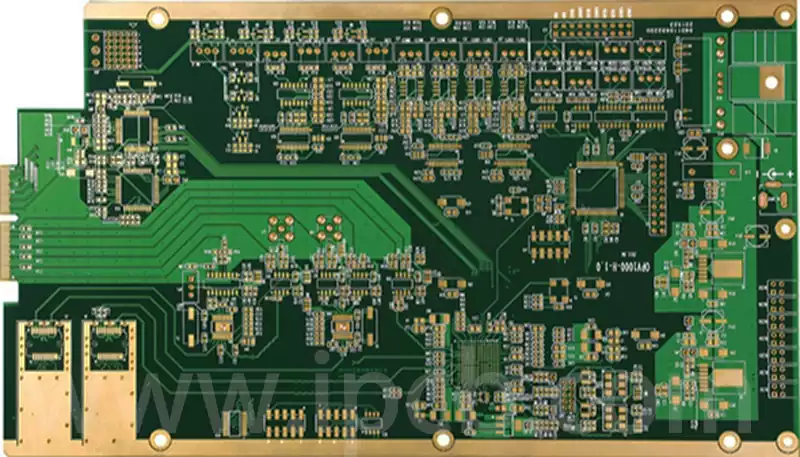
Taking a 4-layer board as an example, the classic configuration is: top layer (RF signal layer), second layer (ground plane), third layer (power/low-frequency signal layer), and bottom layer (digital signal layer). The top layer concentrates RF traces and antenna feedlines, whilst the second layer serves as a complete ground plane, effectively ensuring a stable 50Ω characteristic impedance. The third and bottom layers handle non-RF signals to prevent interference.
For high-layer designs of six layers or more, it is recommended to arrange “signal layers and ground layers” in an alternating pattern to achieve all-round shielding. For example, in a 6-layer PCB designed for a C-band phased array T/R module, the top and bottom layers serve as RF signal layers, with two ground planes positioned in between to sandwich the RF signal layers. This effectively suppresses electromagnetic interference, ensures amplitude and phase consistency across multiple channels, and meets impedance requirements (with variations not exceeding ±5%) across the full temperature range of -40°C to +85°C.
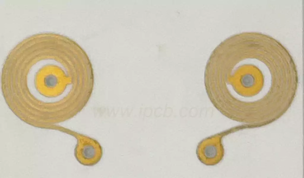
Via treatment directly affects signal transmission continuity and is a key detail in the stack-up design. When changing RF signal layers, blind or buried vias are prioritised to avoid the interference and attenuation caused by through-holes penetrating the entire stack; if through-holes are essential, a back-drilling process must be employed to remove residual stubs—at the 6 GHz frequency band, back-drilling can improve via insertion loss from -0.8 dB to -0.45 dB, yielding a significant improvement.
Ground via density must also be controlled. Placing a ground via every 1.5 mm between the RF signal layer and the ground plane to form a dense array of ground vias can further suppress surface wave propagation and reduce electromagnetic interference. Such attention to detail often determines the upper limit of a product’s performance in high-frequency applications.
Impedance control is a critical detail. The vast majority of RF systems require a characteristic impedance of 50Ω; deviations exceeding ±5% will lead to increased signal reflection, affecting transmission quality. In practice, simulations should be carried out in advance, taking into account substrate parameters, trace width and dielectric thickness, to avoid increased costs associated with later modifications. In terms of routing design, RF traces should be kept as short and straight as possible, avoiding sharp 90-degree bends in favour of 45-degree angles or curved transitions.
Otherwise, signal loss will increase—at the 5 GHz frequency band, a single 90-degree bend can add approximately 5% loss, a factor that is easily overlooked. At the same time, sufficient spacing must be maintained between RF and non-RF traces to minimise crosstalk.
Heat dissipation design must not be neglected. High-frequency RF components generate significant heat during operation; inadequate heat dissipation can lead to a decline in material performance and increased signal attenuation. The standard practice is to place heat-dissipating copper foil beneath heat-generating components and, where necessary, add heat-dissipating vias to conduct heat to the ground plane, ensuring long-term operational stability.
Furthermore, cost control is crucial. Not every layer requires high-end materials; low-loss substrates can be used for the RF signal layer and adjacent ground layers of multilayer RF PCBs, whilst standard FR-4 is employed for other non-critical layers. This approach ensures performance whilst reducing mass production costs, and is a practical technique commonly used in mass production.
The key to designing multilayer RF PCBs essentially lies in finding the optimal balance between performance, reliability and cost. From material selection to stack-up planning, and from via treatment to thermal management, the optimisation of every detail ultimately points towards a single goal: ensuring high-frequency signals travel more stably and facilitating smoother mass production.