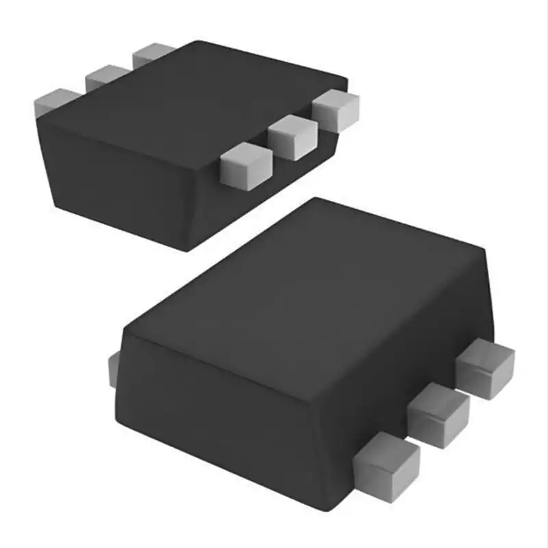
What is a BGA? When dealing with high-density integrated circuits (ICs) – such as microprocessors or complex ASICs – you are likely to encounter ball grid arrays (BGAs). Unlike traditional pin-based packages, this surface-mount technology utilises a full array of solder balls on the underside of the chip, fundamentally resolving the issue of insufficient pin density found in older designs.
In practical applications, the BGA is not merely a ‘better’ packaging option, but an essential choice for modern electronic products. As devices continue to shrink in size and the number of I/O pins keeps increasing, packaging that relies solely on peripheral pins (such as QFP) is no longer sufficient to meet demands. By utilising the entire underside for connections, the ball grid arrays provides more connection points without increasing the package size.
Differences between BGA and traditional packaging
BGA is derived from PGA (Pin Grid Array), but the key difference lies in the fact that pins are replaced by tiny solder balls. These solder balls act as a bridge between the chip and the PCB, providing a reliable electrical connection.
It is important to note that soldering BGAs demands extremely high precision. Automated reflow ovens are typically used, as manual soldering is virtually impractical—the solder balls are small and densely packed. During the reflow process, the surface tension of the molten solder also enables self-alignment, automatically correcting even slight placement deviations.
Common BGA Package Types and Applications
Plastic Ball Grid Array
PBGA is the most common type in the industry and is widely used in devices such as smartphones and routers. It utilises an organic substrate (typically BT resin or FR4), is cost-effective, and is suitable for mass production.
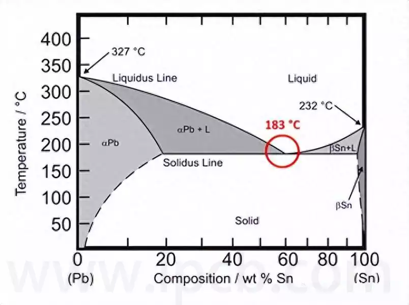
Its greatest advantage lies in the absence of lead bending issues, thereby reducing coplanarity problems during assembly. Most PBGA packages use eutectic solder balls (Sn63/Pb37), which have a melting point of 183°C and are well-suited to reflow solder paste.
Ceramic Ball Grid Array (CBGA)
CBGA is more commonly found in high-reliability applications such as aerospace or medical equipment. Its ceramic substrate offers superior thermal stability and electrical performance compared to organic materials, though it comes at a higher cost.
CBGA typically utilises high-lead solder balls, enabling it to withstand more extreme temperature environments, making it suitable for demanding applications such as engine control units or satellite equipment.
Other ball grid arrays Variants
FC-BGA (Flip-Chip ball grid arrays): The chip is mounted face-down, shortening signal paths, and is suitable for high-performance devices such as CPUs and GPUs.
FBGA (Fine-Pitch ball grid arrays): Ball pitch ≤1 mm, used in ultra-compact products such as wearable devices.
SDGA (Stacked ball grid arrays): Multiple chips are stacked to save space, commonly found in high-performance computing modules.
BGA Packaging Process
1.Substrate Manufacturing
PBGA substrates typically use BT resin/glass fibre as the core material, with copper cladding on both sides. A multi-layer interconnect structure is formed through precision drilling, electroplating and photolithography.
This stage is critical—defects such as blocked through-holes can directly lead to device failure. AOI (Automated Optical Inspection) is typically used for early screening.
2.Chip Mounting and Wire Bonding
After the wafer has been thinned and diced into individual chips, the chips are secured to the substrate using a highly thermally conductive silver adhesive. Plasma cleaning is used to remove contaminants, which could otherwise affect bonding reliability.
Subsequently, wire bonding is performed using gold wires (diameter 0.8–1.0 mil) to connect the chip pads to the substrate pads via ball bonding.
3.Encapsulation, Ball Placement and Reflow
The chip and gold wires are encapsulated and protected using epoxy moulding compound. Solder balls are then placed on the pads on the underside of the substrate (manually for small batches, or using automated equipment for large volumes).
During the reflow process, the solder balls melt to form a stable connection. The peak temperature is typically around 230°C; if too high, this can cause the substrate to warp.
Advantages and Disadvantages of Ball Grid Arrays
Advantages
High density interconnection: Supports hundreds or even thousands of I/O pins, far exceeding the QFP’s limit of approximately 200 pins.
Excellent thermal and electrical performance: Shorter signal paths reduce parasitic inductance and improve high-speed performance; the ball grid array also aids heat dissipation.
Disadvantages
Difficult to inspect: Solder joints are located on the underside of the package, requiring X-ray inspection, which increases quality control costs.
Complex repair: Rework requires specialised equipment (such as hot-air rework stations) and skilled technicians, resulting in higher costs for small batch projects.
Ball Grid Arrays (BGAs) will continue to play a central role in the future. As electronic products evolve towards smaller sizes and higher performance, the balance they strike between density, performance and reliability makes them irreplaceable.