Semiconductor packaging and testing (commonly referred to as ‘packaging and testing’) is a critical final stage in the chip manufacturing supply chain. It involves the post-processing that follows wafer fabrication, protecting the chip’s core circuitry through packaging and establishing electrical interconnections. Through multi-dimensional testing, it screens for good products and verifies performance stability. As such, it directly determines the chip’s ultimate reliability, service life and practical value, making it an indispensable core process for ensuring the successful deployment of chips.
Semiconductor packaging and testing (commonly referred to as ‘packaging and testing’) is a critical final stage in the chip manufacturing supply chain. It involves the post-processing that follows wafer fabrication, protecting the chip’s core circuitry through packaging and establishing electrical interconnections. Through multi-dimensional testing, it screens for good products and verifies performance stability. As such, it directly determines the chip’s ultimate reliability, service life and practical value, making it an indispensable core process for ensuring the successful deployment of chips.
Core Process Flow of semiconductor Packaging and Testing
The complete semiconductor packaging and testing process begins with wafer processing, proceeding through wafer pre-treatment, dicing, die bonding, wire bonding, and molding, before concluding with comprehensive performance testing to ensure quality control. Each step of the process imposes stringent requirements regarding precision and cleanliness.
1.Wafer Pre-processing Steps
Wafer Grinding
Raw wafers fresh from the fabrication process are typically too thick to meet the requirements for subsequent packaging dimensions, thermal management and mechanical structures. Therefore, the backside of the wafer must be ground to reduce its thickness. To prevent damage to the precision circuits on the front side during grinding, a specialised protective film is first applied to the front surface to shield the core chip area. Once the backside grinding is complete and the required thickness for packaging has been achieved, the protective film is removed before proceeding to the next stage.
Wafer Sawing
The thinned wafers are securely affixed to a blue film. Using high-precision cutting equipment, the entire wafer is divided into individual bare chips (dice) along pre-defined scoring lines. Once cutting is complete, the bare chips undergo a thorough cleaning to remove dust and debris generated during the process, thereby preventing subsequent packaging defects caused by residual impurities.
Initial Visual Inspection
The cut bare chips undergo optical visual inspection. High-precision vision equipment is used to detect issues such as chipped edges, scratches, circuit damage and contamination, thereby eliminating defective products at an early stage and reducing the cost of unnecessary processing in subsequent stages.
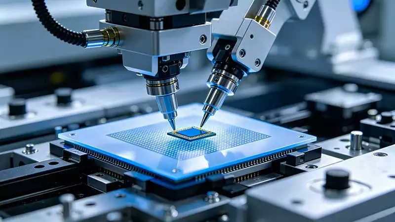
Die Attach
Qualified bare dies are precisely bonded to the corresponding positions on the packaging substrate using a die-bonding machine. The industry generally employs silver paste bonding, which ensures a secure attachment whilst also aiding heat dissipation. Following die attachment, the silver paste is cured to prevent oxidation and cold solder joints. Subsequently, lead bonding is performed to establish the electrical connection between the die and the substrate.
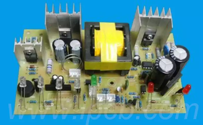
2.The Packaging and Moulding Process
The primary function of packaging is to provide physical protection for the chip, shielding it from external moisture and mechanical damage, whilst also enabling interconnection between the pins. The complete process comprises three stages: pre-packaging preparation, precision packaging, and final sealing and curing.
Pre-encapsulation Preparation
First, a design review is conducted to finalise a suitable encapsulation solution based on the chip’s functionality, number of pins and application scenario. Subsequently, core raw materials such as the encapsulation substrate, gold wires, encapsulation resin and solder are procured, with strict quality control applied. Concurrently, the bare chip and substrate undergo thorough cleaning to remove surface grease and particulates, ensuring a clean encapsulation environment. Finally, gold wire pre-bonding is completed to establish the basic electrical connection.
Core Encapsulation Operations
First, encapsulation resin is evenly applied to the designated area of the substrate to provide cushioning, protection and secure the chip. Next, using high-precision positioning equipment, the bare chip is precisely aligned and placed on the substrate, with strict control over positional and directional accuracy. Subsequently, a heat-curing or UV-curing process is employed to harden the encapsulation resin, achieving a robust bond between the chip and the substrate. Once encapsulation is complete, the assembly is cut and sorted to separate individual encapsulated chips.
Final Encapsulation and Sealing
The encapsulated chips undergo precision cleaning to remove surface dust and processing residues; under suitable temperature and pressure conditions, the encapsulation resin undergoes secondary curing to enhance protective performance; external lead soldering is refined to establish connections between the chip and external circuits; finally, the encapsulation is sealed to isolate the chip from moisture and vapour, preventing internal circuitry failure due to dampness.
3.Comprehensive Performance Testing Process
Once the chip has been encapsulated, it must undergo multi-dimensional, multi-level performance and reliability testing to comprehensively verify its quality. Only products that pass all tests may enter the market. The main test items are as follows:
Functional Testing
As the most fundamental testing phase, this simulates the chip’s actual operating conditions to comprehensively verify the functionality of digital, analogue and mixed-signal circuits. It confirms that the chip’s output, computational and transmission capabilities fully comply with design standards, thereby preventing defective chips from entering the market.
Electrical Characterisation Test
This test precisely measures the chip’s electrical parameters, including rated voltage, operating current, power consumption, output power and impedance. It verifies the stability of the chip’s electrical performance and ensures it meets the power supply and operational requirements of various application scenarios.
Reliability Testing
Conducts rigorous verification of the chip’s long-term operational stability, including temperature cycling tests, high-temperature thermal ageing tests, high-temperature and high-humidity environmental tests, and thermal shock tests. These simulate extreme temperature, humidity and ageing conditions to predict the chip’s service life.
Specialised Performance Testing
These include power consumption testing to assess the chip’s power consumption performance under different operating modes, meeting the requirements of low-power devices; signal integrity testing for high-frequency chips to detect issues such as signal attenuation, crosstalk and distortion; thermal analysis testing to verify the efficiency of the chip’s heat dissipation structure and evaluate thermal performance during high-power operation; and solder joint reliability testing to assess the connection strength and resistance to vibration and impact of the chip’s solder joints, preventing solder joint detachment during long-term use; Visual Inspection: identifies cosmetic defects such as damage to the package casing, bent pins, and air bubbles in the encapsulation.
Trends in Semiconductor Packaging and Testing Technology
With the rapid evolution of the semiconductor industry and the continuous increase in chip integration, the rise in the number of pins and the significant increase in pin density have become the most prominent trends in the packaging and testing sector.
Modern electronic products are becoming increasingly multifunctional, with chips required to handle more functions such as signal transmission, power supply, ground loops, and debugging and calibration; consequently, the number of pins continues to grow. At the same time, as chip manufacturing processes continue to shrink and individual chips integrate more functional modules, pin pitch is constantly decreasing and density continues to rise within the constraints of chip size, compelling continuous innovation and upgrading in semiconductor packaging and testing technologies.
To meet the demands of high-density, highly integrated packaging, the industry has achieved technological breakthroughs in three key areas: packaging structures, bonding processes, and interconnect substrates:
1.Iterative upgrades to new packaging structures: technologies such as BGA (Ball Grid Array) packaging, WLP (Wafer-Level Packaging) and Fan-out packaging are widely adopted, enabling ultra-high-density pin layouts, reducing package volume and enhancing chip integration;
2.The widespread adoption of high-precision micro-soldering technology, with the maturation of processes for microscopic solder joints and ultra-fine pitch soldering, has significantly increased solder joint density and soldering reliability, meeting the demands of precision packaging;
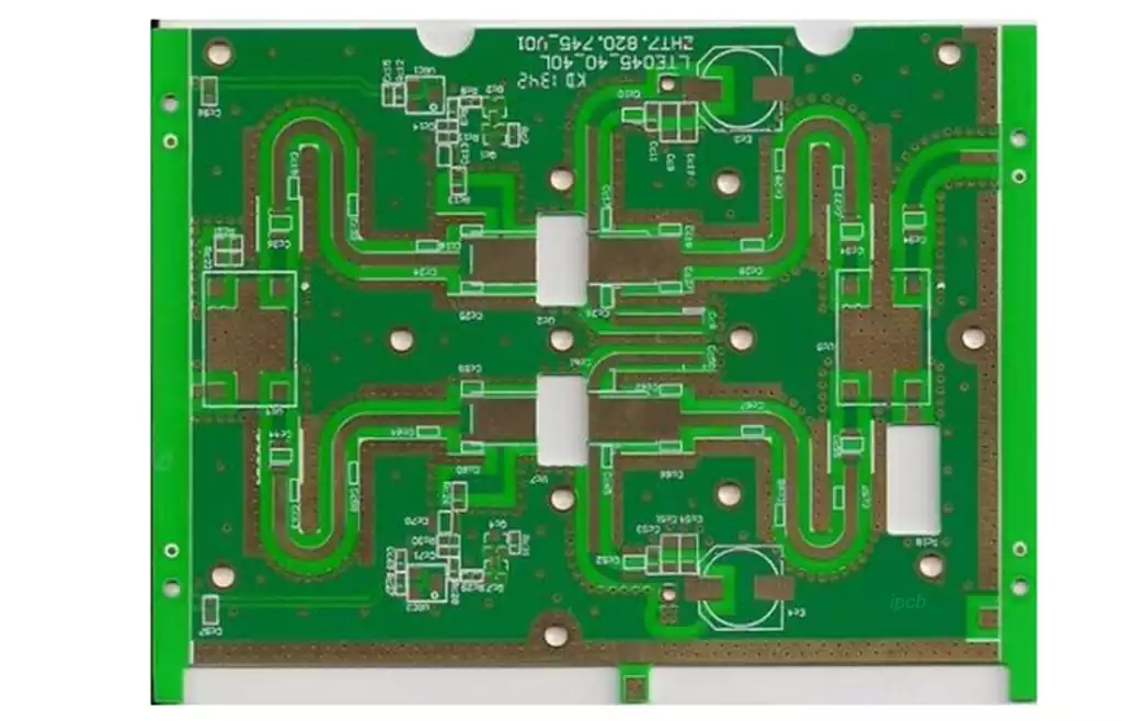
3.Innovations in high-density interconnect (HDI) circuit board technology, with the gradual adoption of multi-layer stacked substrates and high-order interconnect substrates, enabling complex circuit routing to meet the high-speed, high-frequency and high-power operational requirements of high-end chips.
Concurrently, the packaging and testing industry’s requirements for supporting equipment have also risen. Placement machines, wire bonding machines, high-precision test instruments and optical inspection equipment must all possess ultra-high precision, high-speed processing and long-term operational stability to meet the processing demands of micron- and nanometre-scale processes.
Key Application Areas for Semiconductor Packaging and Testing
Communications Sector
Communication equipment such as 5G base stations, smartphones, routers and RF modules places extremely high demands on chip stability and interference resistance. Rigorous packaging and testing processes ensure that communication chips can transmit signals reliably under high-frequency and complex operating conditions, forming the core foundation for the normal operation of communication equipment.
Automotive Electronics
In-vehicle main control chips, sensor chips, power management chips and autonomous driving perception chips are constantly exposed to complex in-vehicle environments involving vibration, extreme temperatures and humidity. High-standard packaging, testing and reliability testing ensure the safety and durability of these automotive chips, which are key to the stable operation of smart and new energy vehicles.
Medical Devices Sector
Core chips in medical sensors, vital signs monitoring devices and precision diagnostic instruments are subject to stringent requirements regarding accuracy, stability and safety. Through rigorous cleanroom controls and reliability testing during the semiconductor packaging and testing phase, the risk of medical incidents caused by chip failure is mitigated, ensuring the precise operation of medical equipment.
Industrial Automation Sector
Industrial controllers, servo drives, industrial sensors, PLC equipment and similar devices must withstand harsh factory environments characterised by dust, vibration and wide temperature ranges. Industrial-grade chips optimised through packaging and testing possess enhanced resistance to interference and ageing, ensuring the continuous and stable operation of industrial automation equipment.
Furthermore, semiconductor packaging and testing are widely applied in consumer electronics, aerospace, artificial intelligence, and new energy sectors. As technology continues to advance, semiconductor packaging and testing processes will evolve further towards miniaturisation, high density and high reliability, providing core support for the upgrading of the entire semiconductor industry chain.
As a key safeguard for the practical application of chips, semiconductor packaging and testing ensures chip quality through standardised process flows and comprehensive testing. With the increasing integration of chips, packaging and testing technologies continue to evolve, adapting to the diverse needs of sectors such as communications, automotive electronics and industry, and providing fundamental support for the stable operation of various electronic devices.