HDI PCB (High-Density Interconnect printed circuit boards) and conventional multilayer printed circuit boards are two types of PCB products in the electronics manufacturing sector that differ significantly in terms of application scenarios and technical standards. As electronic devices rapidly evolve towards miniaturisation, slimness, high performance and high integration, the limitations of traditional multilayer PCB manufacturing processes have become increasingly apparent.
In contrast, HDI PCBs, leveraging advanced manufacturing technologies, have overcome the design and manufacturing constraints of conventional circuit boards. There are significant differences between the two in several key areas, including routing design, physical parameters, structural design, manufacturing processes and cost. The following provides a detailed analysis of the differences across these five core dimensions.
Differences in Routing Density
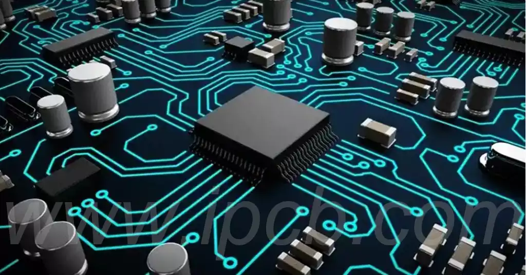
HDI PCBs, relying on proprietary precision interconnection technology, have broken through the routing limitations of traditional PCBs. Given the same board dimensions and substrate area, they can accommodate a greater number of traces and conductive layers, significantly improving the utilisation of board space and achieving ultra-high-density routing layouts.
This high-density routing capability not only effectively reduces the overall volume of the circuit board and shrinks the product’s dimensions but also allows for the integration of more electronic components within a limited space. This greatly enhances the integration and overall performance of electronic products, meeting the design requirements of miniaturised, high-end electronic devices.
Conventional multilayer PCBs, constrained by traditional, established manufacturing processes, face strict technical limitations in routing planning and are unable to achieve fine-grained, high-density circuit layouts. Their circuit layouts feature wider spacing and lower utilisation of the effective routing area; consequently, they can accommodate far fewer circuits and components per unit area than HDI PCBs. Their overall integration capability is relatively weak, making it difficult to meet the R&D and production requirements of compact, high-performance electronic devices.
Differences in Trace Width and Spacing
Trace width and spacing are key indicators of a printed circuit board’s precision, and represent one of the most obvious differences between the two types of boards. HDI PCBs utilise micron-level precision manufacturing processes, enabling extremely fine line widths and minimal line spacing to achieve high-density circuit layout with precision. This ultra-fine circuit design allows for the placement of more functional circuits within a confined board space and the integration of more core functional modules, perfectly adapting to high-precision, multi-functional electronic hardware designs.
Conventional multilayer PCBs have lower manufacturing precision, resulting in wider trace widths and larger spacing between adjacent traces, with a relatively sparse layout. Due to these limitations, their board space utilisation cannot be further improved, and the scale of circuit integration is restricted. Consequently, they can only meet the requirements of conventional, single-function electronic devices and are unsuitable for high-speed, precision-oriented high-end electronic applications.
Differences in Hole Sizes and Through-Hole Processes
In terms of interlayer connection hole design, HDI PCBs possess a clear technical advantage. They abandon the fully through-hole mode of traditional circuit boards and instead utilise blind and buried vias with extremely small diameters to achieve interlayer interconnection in multi-layer circuits. Blind vias connect only the surface layer to the internal layers, whilst buried vias are completely concealed within the board and do not penetrate the surface.
The combined use of these two specialised hole types not only saves a significant amount of board space, reserving ample area for routing, but also simplifies the overall routing logic. At the same time, the non-through-hole structure effectively reduces electromagnetic interference during signal transmission, minimises signal loss, reduces transmission delay, and significantly enhances the stability of high-speed signal transmission.
Conventional multilayer PCBs generally employ traditional large-diameter through-holes to connect layers; these holes are relatively large and must penetrate all layers of the board. This through-hole design not only occupies a significant amount of effective board space and restricts routing layout, but also generates stronger electromagnetic radiation and interference during signal transmission, exacerbating signal loss. This leads to issues such as distortion and delay during high-frequency and high-speed signal transmission, resulting in relatively poor signal transmission performance.
Differences in Overall Structural Design Complexity
HDI PCBs offer exceptional structural design flexibility, enabling the realisation of diverse, highly complex layered structures through advanced manufacturing processes. Specialised designs, such as common stacked microvia structures and vertically stacked interconnect structures, allow for precise interconnection and layered layout of multi-layer circuits. Through three-dimensional, multi-level precision structural design, a vast array of functional circuits can be integrated within an extremely compact PCB footprint, enabling the enhancement and upgrading of product functionality, and perfectly meeting the design requirements for multifunctionality and integration in high-end electronic devices.
The structural design of standard multilayer printed circuit boards is relatively simple and rigid, with an overall hierarchical structure that is straightforward and orderly. They typically employ conventional parallel layering layouts, lacking complex stacked or three-dimensional interconnection structures. With a limited number of circuit layers and poor structural scalability, they offer low design flexibility and can only achieve basic circuit connectivity functions, failing to meet the demands of high-density, three-dimensional circuit integration design.
Differences in Manufacturing Processes and Production Costs
The ultra-high precision characteristics of HDI PCBs place extremely high demands on production equipment, manufacturing processes and the production environment. The production process relies on advanced equipment and techniques such as laser drilling, laser-guided hole positioning, precision micro-etching and interlayer alignment. Furthermore, the entire production process requires stringent control over temperature, humidity, cleanliness and process parameters, resulting in a complex workflow and significant challenges in maintaining yield rates. The investment in multiple high-end processes and equipment, coupled with stringent production control standards, directly results in longer production cycles and higher manufacturing costs for HDI PCBs.
Conventional multilayer PCBs rely on mature, traditional circuit board manufacturing processes. Their production workflows are standardised and simplified, requiring no high-end precision equipment. The threshold for process control is low, production efficiency is high, and yield rates in mass production are stable. Overall production costs are lower, offering significant value for money, making them suitable for the production of high-volume, general-purpose electronic products.
Compared to standard multilayer PCBs, HDI PCBs offer a comprehensive range of core advantages, including high routing density, ultra-fine trace widths and spacing, precision via diameters, flexible and complex structural design, and excellent signal transmission performance. Their sole drawback lies in the stringent process requirements and relatively high production costs.
Thanks to their exceptional integration capabilities and transmission stability, HDI PCBs have now become the core substrate in high-end electronics manufacturing.They are widely used in high-performance electronic products—such as smartphones, laptops, tablets, 5G communication equipment and high-speed servers—where demands for compact size, performance and signal transmission speed are extremely high. Meanwhile, standard multilayer PCBs, leveraging their cost-effectiveness and mature manufacturing processes, continue to be used in various general-purpose consumer and industrial electronic devices. Consequently, the two have established distinct market application profiles.