PCB circuit boards can be categorised by structure into single-sided, double-sided and multilayer boards. Among these, the design of multilayer boards offers a high degree of flexibility, with no strict upper limit on the number of layers. Currently, high-end precision PCBs can exceed 100 layers and are widely used in high-end servers, aerospace and high-end communications. Many people encountering PCB design and manufacturing for the first time may wonder: why are the vast majority of multilayer pcbs on the market even-layered, whilst odd-layered pcbs are extremely rare?
In fact, from a practical perspective, even-layered PCBs far exceed odd-layered ones in terms of market share and frequency of use, and they possess clear advantages in manufacturing processes, product stability and overall cost. The following text will systematically analyse the fundamental reasons why even-layer designs have become the mainstream, and propose feasible solutions for optimising stack-up structures and controlling costs in scenarios where odd-layer boards are essential.
PCB circuit boards can be categorised by structure into single-sided, double-sided and multilayer boards. Among these, the design of multilayer boards offers a high degree of flexibility, with no strict upper limit on the number of layers. Currently, high-end precision PCBs can exceed 100 layers and are widely used in high-end servers, aerospace and high-end communications. In general-purpose applications such as consumer electronics and standard industrial equipment, four-layer and six-layer boards are the most common types of multilayer PCBs.
Many people encountering PCB design and manufacturing for the first time may wonder: why are the vast majority of multilayer boards on the market even-layered, whilst odd-layered boards are extremely rare? In fact, from a practical perspective, even-layered PCBs far exceed odd-layered ones in terms of market share and frequency of use, and they possess clear advantages in manufacturing processes, product stability and overall cost. The following text will systematically analyse the fundamental reasons why even-layer designs have become the mainstream, and propose feasible solutions for optimising stack-up structures and controlling costs in scenarios where odd-layer boards are essential.
Even-layer PCBs offer lower overall costs and more controllable yield rates
From a raw materials perspective alone, odd-layer PCBs appear to have a price advantage as they require one fewer layer of dielectric substrate and copper foil, resulting in slightly lower material costs than even-layer boards of the same specification. However, when analysing the overall production process, the process costs for odd-layer PCBs rise significantly, resulting in a final total cost that is far higher than that of even-layer products, making them less cost-effective.
In terms of inner layer circuit processing for multilayer boards, there is little difference in process complexity or cost between odd-layer and even-layer designs. The primary cost difference lies in the treatment of the outer layer structure and the lamination bonding stages. Even-layer PCBs utilise standardised core lamination processes, featuring symmetrical and regular structures that are well-suited to mature mass production workflows, resulting in high production efficiency and good process tolerance. In contrast, odd-layer PCBs cannot directly employ standard core lamination processes; they require the addition of non-standard core layer bonding steps on top of conventional core lamination, constituting a customised special process.
This non-standard process significantly reduces the mass production efficiency of the production line and adds multiple pre-processing tasks. Prior to formal lamination, the outer core boards of odd-layer PCBs require additional processing such as sanding, levelling and alignment.
This not only extends the production cycle but also substantially increases the risk of defects such as scratches on the outer copper foil, etching deviations in the circuit patterns and misalignment between layers. Consequently, yield rates decline, whilst subsequent rework and scrap costs rise, ultimately resulting in overall production costs that far exceed those of even-layer PCBs.
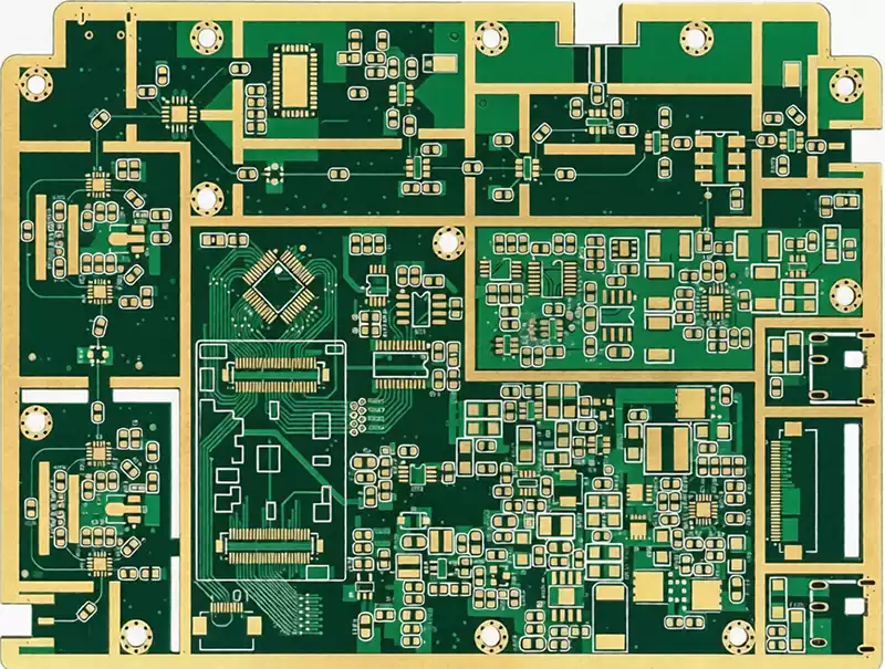
Symmetrical stack-up structures effectively prevent board warping
This is the core reason why odd-layer designs are rarely adopted in the industry. Multilayer PCBs are formed by bonding multiple core layers, dielectric layers and copper foil layers through high-temperature, high-pressure lamination, followed by natural cooling to set the shape. During cooling, different structures generate distinct laminating stresses and shrinkage stresses, and the flatness of the board depends entirely on the symmetry of the stack-up structure.
Even-layer PCBs employ a fully symmetrical stack-up design, with uniform material composition, thickness and stress distribution across all layers. During cooling, these stresses cancel each other out, ensuring maximum board flatness. In contrast, the stack-up structure of odd-layer PCBs is inherently asymmetrical, comprising both core board structures and single-sided copper-clad layers, each with differing coefficients of thermal expansion, cooling contraction rates and laminating stresses. During the cooling phase following high-temperature lamination, these asymmetrical stresses cannot be balanced out, leading directly to warping, bending or deformation of the board.
As board thickness and surface dimensions increase, this structural stress imbalance continues to amplify, significantly raising the risk of PCB bending and deformation. Even if some slightly warped odd-layer boards pass basic factory inspections, they present numerous hidden risks for subsequent assembly, reducing processing efficiency in downstream operations.
During SMT placement, component soldering and final assembly, warped circuit boards require specialised calibration equipment and special processes. This not only increases equipment and labour costs but also readily leads to issues such as component placement deviations, cold solder joints and solder joint failure, severely affecting assembly precision and product reliability.
Taking the IPC-600 standard as an example, the warpage of a four-layer even-layer PCB can be consistently controlled within 0.7%, fully meeting the requirements of precision SMT production; whereas a three-layer odd-layer board of the same size and process is highly prone to exceeding warpage limits, making it difficult to adapt to standardised SMT mass production processes.
Consequently, the industry generally adheres to a design principle: even if a product’s functionality requires only an odd number of layers for routing, it is designed as a ‘pseudo-even-layer’ board by adding redundant layers—for example, converting a five-layer board to a six-layer board, or a seven-layer board to an eight-layer board—thereby fundamentally eliminating the risk of warpage through symmetrical stacking.
Layer Balancing and Cost Optimisation Solutions for Odd-Layer PCBs
1.Adding a redundant signal layer to optimise the stack-up structure
This approach is most cost-effective for designs where the number of power layers is even and the number of signal layers is odd. Designers can add a blank redundant signal layer to the original odd-layer routing scheme. This layer requires no routing and does not alter the original circuit functionality; it is used solely to balance the overall stack-up, ensuring symmetrical stress distribution across the board. This approach adds virtually no extra material or manufacturing costs; on the contrary, it simplifies the manufacturing process, shortens lead times, and significantly improves board flatness and product quality.
2.Adding a Power Ground Layer to Balance Board Stress
In cases where the number of power layers is odd and the number of signal layers is even, an optimisation scheme involving the addition of a power ground layer can be adopted. Specific procedure: Without altering the original circuit layout or stack-up parameters, add a ground layer at the centre of the stack-up structure.
During design, routing can first be completed according to the original odd-layer structure, followed by duplicating the central layer and labelling the remaining layers. The electrical performance of this solution is essentially equivalent to thickening the copper foil of the existing ground layer; it achieves stack-up symmetry and eliminates stress deviations whilst ensuring ground performance and electrical stability.
3.Adding a blank signal layer at the centre to accommodate special circuit scenarios
Suitable for special scenarios such as microwave circuits and mixed-dielectric circuits (where the dielectric constants of the board layers differ). The core procedure involves first completing the full routing design for the odd-numbered layers, then adding a single blank signal layer at the exact centre of the stack-up. This redundant layer at the centre maximally offsets the stress differences caused by the asymmetrical structure, thereby reducing the risk of warping and deformation at the source and significantly improving the production yield and operational stability of PCBs for specialised circuits.
Considering the overall process complexity, product stability, production costs and suitability for mass production, even-layer PCBs, with their symmetrical stack-up structure, can perfectly avoid warping issues. They feature mature processes, high mass production efficiency and low overall costs, making them suitable for the usage requirements of the vast majority of electronic devices. This is the fundamental reason why even-layer PCBs are the mainstream choice for multilayer boards. Conversely, due to structural flaws, complex processes and poor stability, odd-layer PCBs are only suitable for a few specialised custom scenarios. Furthermore, their laminate structure must be optimised by adding redundant layers to meet mass production and operational standards.