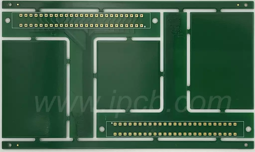
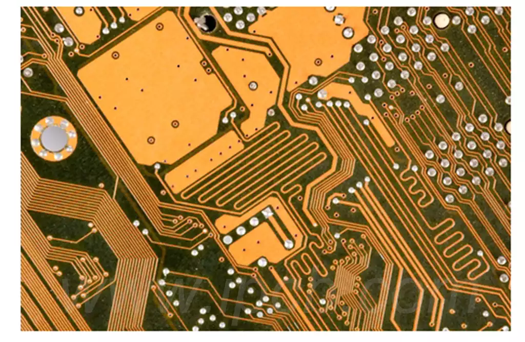
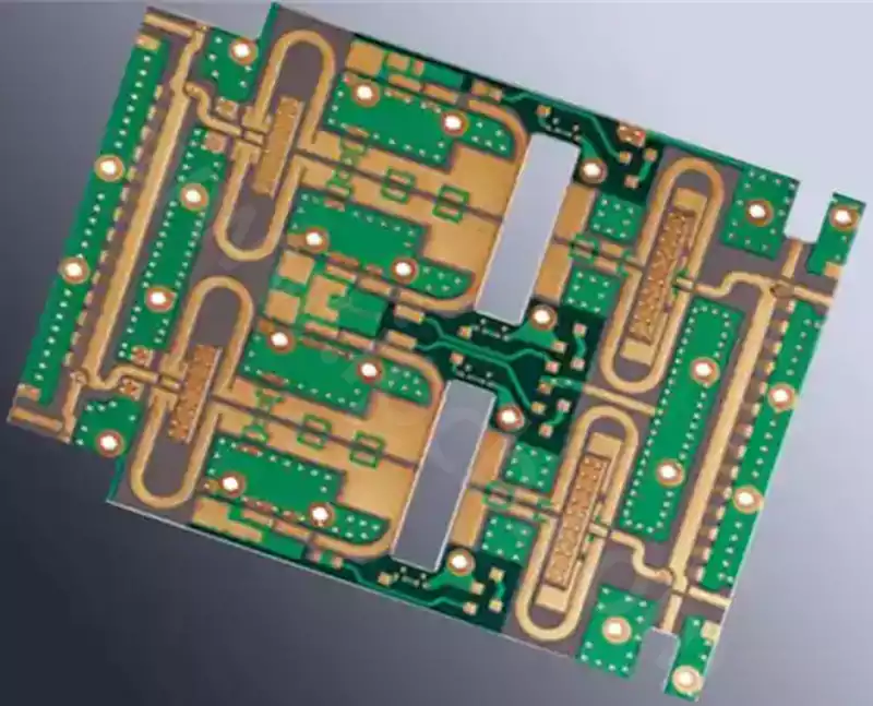
A multilayer ceramic substrate is a circuit substrate formed by alternately stacking multiple conductive wiring layers and insulating dielectric layers, followed by integrated co-firing into a single structure. Because of its layer-by-layer construction, it is also commonly referred to as a laminated ceramic substrate. One of the greatest advantages of this architecture is its ability to distribute signal traces, power planes, and ground layers across different layers of the substrate. This not only significantly increases routing density but also helps minimize signal crosstalk and electromagnetic interference, thereby enhancing overall circuit stability and reliability.
Within today’s circuit board industry, resin-based multilayer substrates, particularly those built on FR-4 epoxy resin and polyimide materials, continue to dominate the market. However, as advanced electronics and equipment designed for extreme operating environments become increasingly common, multilayer ceramic substrates have rapidly emerged as a major focus of research and industrial adoption due to their superior overall performance.
The manufacturing principles of these two substrate technologies differ fundamentally. Ceramic substrates use inorganic ceramic materials, such as alumina, as the base material. After multiple layers are stacked together, the entire structure is co-fired at high temperatures to form a monolithic substrate. Depending on the firing temperature and material system employed, ceramic substrates are generally classified into two categories: Low-Temperature Co-Fired Ceramics (LTCC) and High-Temperature Co-Fired Ceramics (HTCC).
Compared with conventional resin-based substrates, ceramic substrates offer significant advantages in high-temperature resistance, chemical resistance, hermeticity, and dimensional stability. These characteristics make them particularly suitable for demanding operating conditions involving high temperatures, high voltages, vacuum environments, corrosive chemicals, and plasma exposure. Owing to their exceptional long-term reliability, ceramic substrates have become widely used in sensors, medical analytical instruments, power electronic devices, aerospace systems, and other high-performance applications.
From an application perspective, resin-based laminated substrates and multilayer ceramic substrates occupy distinctly different positions. Resin substrates excel in large-scale mass production. Supported by highly mature manufacturing processes, they enable extremely low production costs for high-volume consumer electronics such as smartphones. In contrast, multilayer ceramic substrates demonstrate clear advantages in low- to medium-volume production, high-layer-count circuit designs, and applications where reliability is a primary concern.
This distinction becomes especially apparent in environments involving plasma processing, vacuum operations, exposure to aggressive chemical media, or applications that demand exceptional repeatability and long service life. In these sectors, purchasing decisions are increasingly driven not by initial acquisition costs but by long-term operational stability and total lifecycle costs. As a result, the value proposition of ceramic substrates becomes even more compelling.
The differences between these two substrate technologies extend beyond their applications to their manufacturing methods, materials, and performance characteristics. Multilayer ceramic substrates are produced using ceramic green tapes that are laminated and subsequently co-fired at elevated temperatures. Alumina and other inorganic ceramic materials serve as the substrate body, while conductors are typically formed using specialized metals such as tungsten, molybdenum, silver, or precious metals. LTCC materials are generally fired at approximately 900°C, whereas HTCC substrates may require firing temperatures approaching 1,600°C. These high-temperature manufacturing processes impart excellent thermal conductivity, heat resistance, corrosion resistance, and hermetic sealing capabilities, enabling reliable operation under extremely demanding conditions.
By comparison, resin-based substrates are manufactured by building conductive layers sequentially onto a resin-based dielectric structure. The most common material combination consists of FR-4 epoxy resin and copper foil, with processing temperatures typically remaining around 200°C. This approach allows finer line widths and spacing, thinner overall constructions, and greater flexibility for multifunctional integration. As a result, resin-based substrates remain the preferred solution for smartphones, laptops, consumer communication devices, IoT products, and other mainstream electronics.
However, resin substrates exhibit clear limitations in heat resistance, chemical durability, and hermetic performance. Consequently, they are best suited to relatively benign operating environments. While ceramic substrates generally carry a higher unit cost and are therefore more appropriate for high-value, specialized applications, resin substrates benefit from lower production costs and broad scalability. Nevertheless, as circuit complexity and layer counts increase, the overall cost advantages of resin-based solutions can diminish significantly.
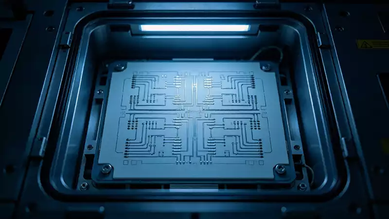
The ongoing trend toward higher integration density and multifunctional electronic systems has led many advanced applications to demand near-zero failure rates and stable operation across a wide range of environmental conditions. Multilayer ceramic substrates were developed specifically to address these requirements. Their manufacturing process involves forming conductive features such as electrodes and vias on ceramic green tapes, stacking multiple layers together, and then co-firing the entire assembly into a unified structure. This approach allows the intrinsic physical and chemical properties of ceramic materials to be fully utilized, resulting in performance levels that align with the requirements of advanced precision equipment.
From a thermal perspective, HTCC substrates are capable of operating in environments exceeding 1,000°C, making them ideal for high-temperature industrial equipment and high-power electronic systems. Their exceptional resistance to chemical attack allows them to withstand exposure to a wide range of acidic and alkaline media, making them highly suitable for medical diagnostics, chemical analysis, and other applications involving aggressive substances. Their excellent hermeticity supports vacuum environments and sealed-package designs, while their low sensitivity to temperature and humidity variations ensures outstanding dimensional stability during long-term operation. Electrically, ceramic substrates provide high insulation resistance, low dielectric losses, and strong immunity to signal interference, enabling reliable transmission of high-frequency and low-amplitude signals.
The choice of conductor materials also varies between ceramic substrate technologies. HTCC substrates typically employ high-melting-point metals such as molybdenum and tungsten to withstand the elevated firing temperatures. Some products require additional metallization or plating processes after firing. Certain proprietary HTCC solutions, such as Nikko’s Hi-Cerafill® series, utilize platinum conductors, which offer superior oxidation resistance and eliminate the need for post-firing electroplating.
LTCC substrates, on the other hand, primarily use silver or silver-palladium alloy conductors. Depending on application requirements, some products may also incorporate gold plating. Because silver-based conductors offer excellent electrical conductivity, LTCC substrates perform particularly well in high-frequency signal transmission and fine-line circuit designs. They are widely used in RF and microwave applications and can integrate passive components such as resistors directly within the substrate structure. The lower firing temperatures of LTCC technology also allow certain electronic components to be co-fired with the substrate, helping simplify assembly processes and reduce manufacturing complexity. Furthermore, the glass content incorporated into LTCC dielectric materials lowers the dielectric constant, improving signal transmission performance.
As the two primary categories of multilayer ceramic substrates, HTCC and LTCC serve different application requirements due to their distinct material systems, firing processes, and conductor technologies.
HTCC technology relies on firing temperatures of approximately 1,600°C and is typically based on high-purity alumina substrates combined with high-melting-point conductor materials such as molybdenum and tungsten. Certain advanced designs employ platinum conductors, allowing firing in ambient air and simplifying the manufacturing process. Once fired, HTCC substrates exhibit exceptional mechanical strength, high-temperature durability, moisture resistance, chemical resistance, and hermetic performance. These attributes make them particularly well suited for medical analytical equipment, aerospace systems, plasma-processing equipment, and high-vacuum electronic packages.
LTCC technology, by contrast, utilizes firing temperatures around 900°C and is primarily paired with highly conductive silver or silver-palladium conductor systems. The excellent conductivity of these materials enables superior performance in RF circuits and high-frequency applications while supporting highly integrated multilayer designs. LTCC substrates can also accommodate embedded passive components and co-fired device integration, further reducing assembly complexity. The principal limitation of LTCC technology lies in the susceptibility of silver-based conductors to oxidation. Consequently, many LTCC products employ surface finishes such as nickel or gold plating to enhance long-term corrosion resistance and maintain electrical stability.
The advantages and limitations of multilayer ceramic substrates are highly application dependent. Their most significant strengths include exceptional thermal resistance, outstanding chemical durability, high mechanical rigidity, excellent hermetic sealing performance, and remarkable long-term reliability. These properties allow ceramic substrates to maintain structural integrity and electrical performance in environments where conventional materials would degrade, deform, or fail. Ceramic substrates also facilitate the integration of cavity structures for sensor packaging and thermal management solutions, while their extremely low moisture absorption ensures stable electrical characteristics even at high frequencies.
At the same time, ceramic substrates possess certain inherent limitations. Ceramic materials are naturally brittle and exhibit lower impact resistance than resin-based alternatives, requiring careful mechanical design to mitigate potential damage. In addition, via sizes and routing densities are generally less refined than those achievable with advanced resin-based substrates, making ultra-fine routing and extremely high layer counts more challenging. The use of precious-metal conductors in some designs can further increase manufacturing costs, particularly for products requiring large conductive areas. Consequently, in cost-sensitive consumer electronics applications, the performance advantages of ceramic substrates often exceed actual requirements, limiting their adoption primarily to premium products with stringent reliability demands.
Thanks to their unmatched ability to withstand extreme environments and deliver long-term operational stability, multilayer ceramic substrates have become an indispensable enabling technology for advanced equipment manufacturing and cutting-edge scientific research. Although challenges related to impact resistance and ultra-fine circuit density remain, ongoing advances in ceramic materials, conductor technologies, and co-firing processes continue to improve their capabilities. As these innovations progress, multilayer ceramic substrates are expected to play an increasingly important role in the next generation of high-performance electronic systems.