The Underlying Architecture of Stereo Microscopes and Digital Video Microscopes
In the rework workshops of the electronics industry, microscope for repair PCB have undergone a profound technological evolution from traditional purely optical stereo microscopes to modern high-frame-rate digital video microscopes. These two architectures follow completely different physical imaging logics when capturing the surface morphology of microscopic circuit boards.
The Greenough and Concurrent Orbit (CMO) dual-mechanical purely optical stereo microscopes remain the uncrowned king for high-end motherboard wiring and micro-soldering engineers. Their core value lies in providing a true three-dimensional stereo depth perception. In actual optical topologies, there are two main schools of thought: the Greenough optical path architecture: The microscope has two completely independent imaging optical paths within it, at a certain angle (typically 10° to 12°), sharing the same binocular objective lens front end.
The ingenuity of this design lies in the fact that the two light paths simulate the microscopic parallax of the human left and right eyes when observing objects from different angles. Because the light paths inherently have an angle, they produce an extremely strong and layered three-dimensional microscopic stereoscopic vision. When an engineer touches the sidewall pad of a 01005 packaged capacitor with a soldering iron tip, the Greenau light path allows them to perceive the vertical distance between the soldering iron tip and the solder with extreme precision, thus eliminating wafer scratches caused by blindly inserting the soldering iron. The Common Main Objective (CMO) architecture: It collects a parallel beam of light through a large main objective lens that is completely perpendicular to the objective lens plane, and then splits the beam into two independent zoom systems. The CMO architecture almost completely eliminates optical distortion across the entire magnification range and is extremely suitable for high-end optical accessory expansion (such as introducing coaxial illumination, beam splitter video connectors, etc.). However, because its light path is parallel, its inherent three-dimensional depth perception is slightly inferior to the Greenau architecture.
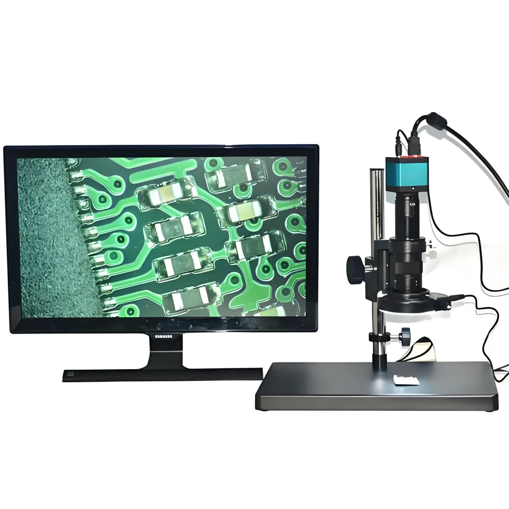
The battle for sensor throughput and zero latency in digital video microscopes: With the widespread adoption of 4K ultra-high-definition image sensors and ultra-large screens, digital video microscopes have become the mainstream for high-density production line inspection and batch rework due to their ability to completely liberate engineers’ necks and retinas. However, for real-time manual soldering repair, digital microscopes face a fatal physical weakness—image capture and display latency. When the CMOS sensor of a digital camera captures the moment the solder melts on a microscopic trace, the image data must undergo high-speed arrangement through ISP (Image Signal Processor) algorithms such as pixel binning, automatic white balance, and noise reduction before finally being transmitted to the monitor via an HDMI interface.
If the total latency of this process exceeds 60 milliseconds, the image seen by the engineer on the screen will become noticeably disconnected from their physical hand movements. This subtle time lag can cause a strong sense of dynamic dizziness, making precise soldering repair extremely difficult. Therefore, the core technology of a qualified digital rework microscope is not simply the pixel count, but its data bus throughput and frame rate. Top-of-the-line industrial-grade video microscopes fully utilize native uncompressed 4K @ 60fps full-motion streaming output, coupled with a minimalist, hardware-level, zero-buffered ISP chip topology. The charge signal is directly converted and ejected onto the HDMI signal cable the instant it leaves the CMOS pixel, suppressing end-to-end latency to below 10 milliseconds. This results in a silky-smooth, ghosting-free display on the monitor screen, achieving ultimate physical hand-eye synchronization.
The Material Science Balance Between Working Distance and Depth of Field.
In the optical design of a microscope for repair PCBs, there are two core parameters that are diametrically opposed and fiercely contested in physics: working distance (WD) and depth of field (DoF).
The Lifeline of Mechanical Avoidance: Why Repair Microscopes Require Extreme Working Distances. For purely biological microscopes, specimens are sandwiched between thin slides, with the objective lens typically only a few millimeters or even a fraction of a millimeter away from the specimen. However, in the repair of complex power motherboards or mobile phone circuit boards with large shielding covers, this distance is devastating. Repairing means engineers must simultaneously cramm the hot air gun nozzle, high-frequency soldering iron tip, precision flying wire tweezers, and rosin solder wire into the narrow three-dimensional space between the microscope objective and the motherboard surface.
If the microscope’s physical working distance is less than 80 mm, the 350-degree Celsius heat from the hot air gun will directly bombard the expensive front lens of the objective, causing the anti-reflective coating to instantly crack and peel off chemically, and even melting and deteriorating the internal optical cement. Therefore, the initial working distance of industrial-grade repair microscopes is generally required to be 100 mm to 110 mm.
To achieve this, optical designers must introduce large-aperture, special low-dispersion (ED) long-working-distance auxiliary objectives (typically 0.5x or 0.7x reduction lenses) at the front of the zoom system. This not only provides ample “physical movement corridors” for various repair tools but also doubles the microscope’s field of view, allowing engineers to maintain macroscopic control even in microscopic environments.
Microscopic Depth of Field: Combating Visual Fatigue Caused by Frequent Focusing Depth of field refers to the vertical thickness of the motherboard surface that allows for clear imaging in the longitudinal dimension without changing the microscope’s focal length. A mobile phone motherboard is not a flat plane; the towering electrolytic capacitors, medium-height BGA chips, and bottom-mounted resistors and capacitors are arranged vertically, creating a “microscopic valley” with a drop of several millimeters. If the microscope’s optical digital aperture (NA) is set too large, the depth of field becomes extremely thin (even only tens of micrometers).
This means that when an engineer can clearly see the silkscreen on the top of a BGA chip, the solder pads on the bottom of the chip become a blurry ghost image; if he raises the tweezers slightly, the tweezers tip immediately goes out of focus. To see clearly at different heights, he had to manually turn the focusing wheel on the main unit year-round. To free engineers from the tedious mechanical labor of frequent focusing, rework-grade microscopes must embed a high-precision, dynamically adjustable aperture (Iris Diaphragm) within the optical path. By appropriately reducing the aperture diameter, stray light flow at the edges entering the optical path is physically limited, forcibly lengthening the vertical depth of field using the pinhole imaging principle. This allows the entire board to maintain sharp and clear resolution simultaneously, whether viewing mountains or valleys, within a vertical drop of 2 to 3 millimeters. This not only allows for seamless soldering and wire connection processes but also significantly reduces deep eye dryness and visual fatigue caused by frequent focusing of the ciliary muscle in the human retina.
Coaxial Illumination and All-Around Anti-Static Failure
In the microscopic world of a circuit board, the reflective optical characteristics of various material surfaces are extremely extreme and challenging. The mirror-smooth bare copper pads, the IC surface with its highly reflective silicon wafer, the rough, uneven light-absorbing solder resist, and the hemispherical, highly reflective solder joints are all mixed together. If the lighting system is poorly designed, this microscope for repair PCB can become an “electromagnetic flash bomb” creating visual obstruction.
Ring Light and Polarization: Photonic Purification. Traditional direct-light LED ring lights, while bright enough, cause severe total internal reflection when the light strikes the smooth, highly reflective surface of the spherical solder joints. This creates a white, detail-less “glare” on the microscope eyepiece or image sensor. Under this glare, microscopic defects such as poor solder joints, pinholes, or microcracks hidden within the solder joints are completely masked, causing repair personnel to miss critical, invisible physical defects.
To eliminate glare, modern high-precision repair lighting systems incorporate a physical polarization system and multi-angle diffuse reflection technology. A circular polarizer is added to the front of the LED ring light, while an analyzer is screwed into the front of the microscope objective. When natural light passes through the polarizer and becomes directionally polarized, striking the uneven circuit board substrate, the insulating solder mask and substrate asymmetrically diffuse reflect the light, disrupting its polarization direction; while smooth metal solder joints reflect the polarized light back intact.
By rotating the analyzer at the microscope’s front, the specularly reflected light with strong directional glare can be precisely filtered and intercepted, allowing only diffusely reflected photons with microscopic geometric details to pass through the optical system. Under the microscope, the originally glaring metal solder balls instantly become smooth and lustrous, revealing the microscopic metal grain texture on their surface, and even the micron-sized rosin residue (flux residue) can be meticulously resolved.
As a mechatronic tool that operates in constant proximity to delicate semiconductor components, a microscope’s physical materials, if not properly protected, can become a dangerous “high-voltage electrostatic reservoir.” In dry, cleanroom environments, friction from engineers’ clothing and airflow cause the microscope’s exposed plastic casing and metal support to accumulate free charges.
Without robust ESD protection, when an engineer adjusts the microscope tube angle or pushes the microscope head over an exposed ultra-large-scale integrated circuit (such as a mobile phone CPU wafer), the accumulated high-voltage static electricity can travel through the casing and air, causing a momentary electrostatic discharge (ESD) breakdown on the chip pads below. The surge of thousands of volts released within a microsecond can completely melt and burn through the silicon dioxide insulating gate layer, which is only tens of nanometers thick, inside the microprocessor, creating an atomic short circuit.
This explains why many motherboards, despite having their wiring correctly installed under a microscope, still fail to power on, revealing the core chip to be inexplicably dead – a fundamental hardware failure mechanism. To eliminate this silent killer, the entire physical coating of a top-tier microscope for PCB repair undergoes rigorous modification and tuning with ESD dissipative materials. The surface is coated with a special polymer paint doped with nanoscale conductive carbon fibers or conductive metal oxides, ensuring the surface resistance is maintained within the perfect dissipation range of 10^6 to 10^9 ohms.
Simultaneously, the microscope’s omnidirectional mechanical metal boom stand, focusing bracket, and base are all physically and securely connected to the external central grounding terminal (GND) via multi-point parallel thick wires. This ensures that any minute charge generated under any frictional environment is mercilessly conducted to ground within a millisecond, creating an absolutely safe electrostatic immune protection network for the entire multi-layered precision circuit board at the microscopic level.
Mechanical Stability of Heavy-Duty All-Metal Mechanical Stands
After understanding the microscopic mechanisms of the optical path, zero-delay sensors, and anti-static coatings, the ultimate physical foundation supporting the high efficiency of these core technologies in routine rework is directly embedded in the microscope’s external mechanical stand.
The microscopic amplification effect of mechanical vibrations, combined with the vibration damping mechanics of the heavy-duty articulated arm, means that under high-magnification optical magnification of 30x or even 90x, any minute vibration in the physical world will be magnified proportionally by tens of times. If the microscope is equipped with a traditional, simple tabletop stand, then the movement of people at adjacent workstations in the rework room, the roar of air pumps, and even the slight eccentric vibration of the cooling fan on the table will be relentlessly transmitted to the microscope lens through the tabletop. In the eyepiece or monitor screen, this will cause the entire microscopic motherboard to experience frantic, high-frequency physical shaking and dizzying displacement.
In such shaky conditions, engineers can’t even align the tip of tweezers, let alone perform micron-level chip adhesive removal and gold wire bonding operations. To maintain a stable image, high-end rework stations must be equipped with heavy-duty dual-arm ball bearing boom stands. These stands typically weigh tens of kilograms, with the core crossbar constructed from high-rigidity solid chrome-plated hard steel, internally embedded with high-precision industrial-grade linear rolling bearings. Their high-density physical weight and perfect dynamic balance design form a natural low-pass mechanical filter, capable of instantly absorbing and offsetting high-frequency micro-vibrations from the ground.
More importantly, this boom, tens of centimeters long, provides an extraordinary degree of freedom in three-dimensional space. Whether facing a massive automotive central gateway motherboard half a meter wide or an oddly shaped industrial inverter base, engineers can easily suspend the microscope head directly above any dead corner of the motherboard with a gentle push, without occupying any valuable desktop physical operating space, achieving true “three-dimensional space liberation”.
Microscopic Elimination of Gear Drive Dead Zones: The rigid control of a precision focusing bracket in a microscope relies entirely on the conventional rack and pinion mechanism within the focusing bracket for longitudinal focusing. Over years of frequent use, mechanical wear inevitably leads to minute backlashes and idle travel between the metal gear teeth. If the focusing bracket lacks a backlash-eliminating design, when an engineer wants to finely adjust the focus by 10 micrometers to see the root of the flying line, turning the knob may result in no physical displacement of the microscope head due to the gear dead zone.
However, if too much force is applied, the microscope head may suddenly lurch downwards by tens of micrometers, causing the focal plane to drift instantly. To overcome this mechanical weakness, professional rework-grade focusing brackets must be equipped with a bidirectional spring-loaded tension adjustment mechanism. Through internal high-rigidity disc springs, a constant, opposite-direction micro-mechanical pressure is applied to the transmission gears year-round, forcibly compressing the microscopic fit clearance between the gears and rack to an absolute zero physical dead zone. Combined with high-viscosity synthetic fluorine damping grease, every extremely slight fingertip twist by the engineer is 100% losslessly converted into smooth, precise micrometer-level vertical movement of the camera head, elevating the manual focus control precision of the entire high-density rework production line to the pinnacle of semiconductor fine-tuning.