Demystifying the Core Packaging and Thermoelectric Failure of Active Semiconductor Components
In the macroscopic layout of PCB board parts, active components are the core brain and power heart of the entire electronic system. They possess the nonlinear electrical characteristics of their internal transistor structures, enabling amplification, switching, and logic modulation of electrical signals. However, they also stand at the forefront of overall board power consumption and thermal stress failure.
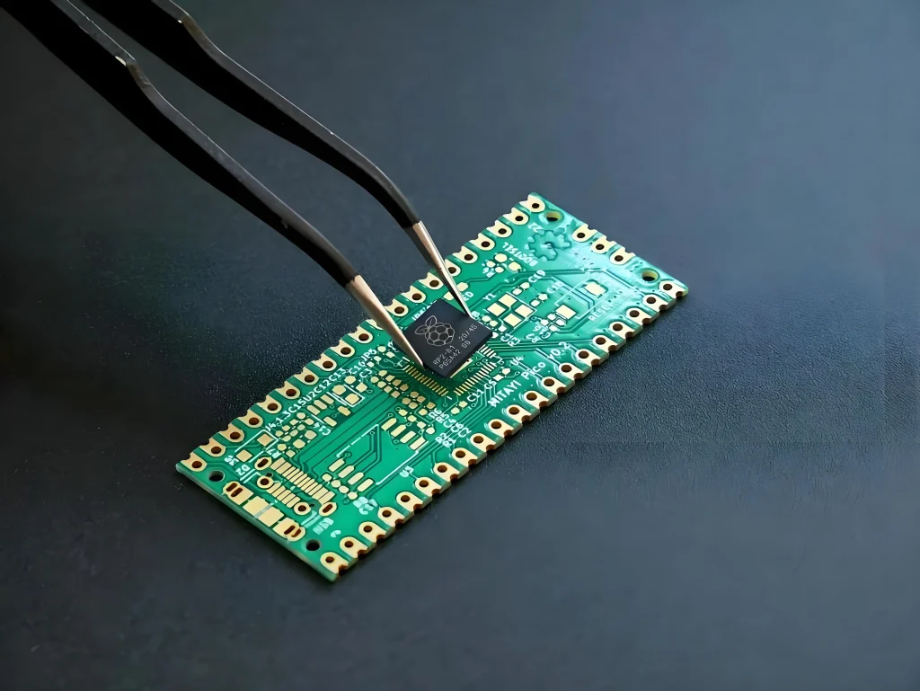
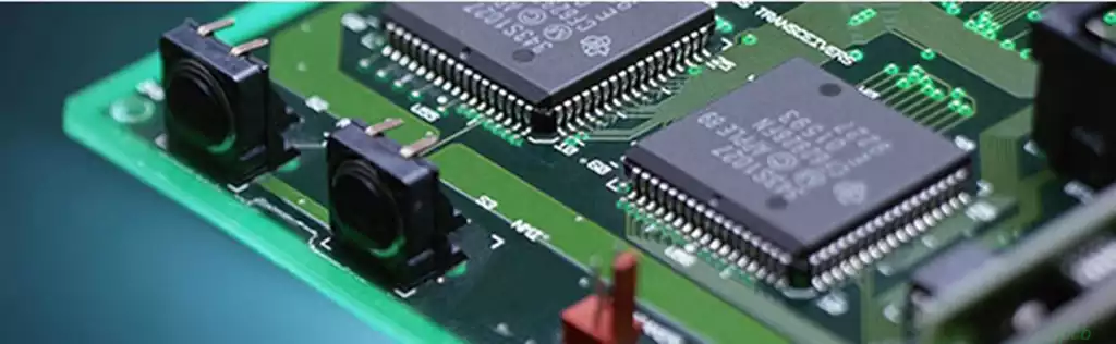
Wafer-Level Packaging (WLCSP) and Ball Grid Array (BGA) Microscopic Interconnection in Modern Smart Devices or High-Performance Servers: Central Processing Units (CPUs), Graphics Processing Units (GPUs), and Microcontrollers (MCUs) have completely abandoned traditional leadframe packages with pins (such as QFP and SOP), shifting to extremely high-density Ball Grid Arrays (BGAs) and Wafer-Level Chip-Scale Packaging (WLCSP). The physical essence of this packaging is to directly lead the electrodes from the bottom of the semiconductor silicon wafer (die) to a matrix of solid solder balls at the bottom of the package using micrometer-scale gold or copper pillars.
When these components are reflow soldered onto the motherboard surface, hundreds or even thousands of tiny solder balls, each only 0.25 mm in diameter, instantly melt and eutectic, directly connecting the chip to the motherboard’s inner layer micro-blind vias. This structure microscopically eliminates the enormous parasitic inductance of traditional metal pins, allowing high-frequency clock signals of tens of gigahertz to pass through without loss. However, BGA solder balls face extremely severe mechanical fatigue failure during their service life.
The linear coefficient of thermal expansion (CTE) of silicon wafers is extremely low (approximately 3 ppmC), while the underlying FR4 resin substrate has a CTE as high as 15 ppmC. As the chip repeatedly switches between full-load operation and standby, the solder ball layer is subjected to severe microscopic shear stress due to uneven heating over many years. If the PCB manufacturer’s plating layer contains minute voids, or if the reflow profile is inaccurate, preventing the formation of a sufficiently thick (ideally 1 to 3 micrometers) intermetallic compound (IMC, such as Cu6Sn5 or Cu3Sn) layer between the solder balls and the motherboard pads, the outer solder balls at the bottom of the chip will develop hidden microcracks and break after dozens of thermal cycles. This can lead to bus data loss and cause the entire system to crash unexpectedly.
Power metal-oxide-semiconductor field-effect transistors (MOSFETs) and diodes, as absolute power control components within the power management unit (PMIC) and inverter, act as high-frequency electronic switches. At the microscopic level, each switching transition of a MOSFET is accompanied by a dramatic accumulation and dissipation of charge in the semiconductor’s internal conductive channel. In kilowatt-level ultra-fast charging or motor drive circuits, these switching components undergo hundreds of thousands of on/off cycles per second.
Because power semiconductors inherently possess on-resistance and reverse recovery charge, a massive transient heat flux density accumulates between the drain and source at each switching instant. To prevent these expensive power components from experiencing physical thermal breakdown due to a surge in intrinsic carriers when reaching the 175°C junction temperature limit, the supply chain for modern high-end PCB board components must completely restructure the thermal conductivity pathways on their undersides.
Power transistors in packages such as D2PAK and DFN inherently have a large, exposed metal drain heatsink on their underside. During assembly and routing, engineers must densely arrange dozens of thermal vias penetrating the motherboard directly beneath this pad, or directly introduce advanced thermoelectric separation technology to forcibly draw the Joule heat accumulated inside the component vertically to the underlying layer through pure metal channels, completely eliminating the risk of localized thermal stress bursting.
The Parasitic Trap and Dielectric Degradation of Passive Components
If active components are the commanders of the battlefield, then passive components, consisting of resistors, capacitors, and inductors, are the steel infantry, making up over 85% of the total. Under extreme conditions of ultra-high frequency and high voltage, these seemingly simple parts reveal their hidden electrical properties in surface materials science.
The Piezoelectric Effect and Phonon Implosion of Multilayer Ceramic Capacitors (MLCCs) Multilayer ceramic capacitors (MLCCs) are the most numerous decoupling and filtering components on a multilayer board. Their microstructure resembles a nanoscale layered cake composed of dozens of alternating layers of metal inner electrodes and barium titanate (BaTiO3) ceramic dielectric layers.
Barium titanate is a strong dielectric with an extremely high dielectric constant, but it possesses an extremely challenging physical property in crystallography—ferroelectricity and the piezoelectric effect. When the CPU on a mobile phone motherboard or computing board undergoes high-load dynamic current switching, the voltage on the power supply rail generates high-frequency micro-amplitude ripples. When these high-frequency AC ripples impact the interior of MLCC components, the barium titanate lattice undergoes micrometer-level physical deformation and mechanical stretching in response to the alternating electric field strength.
This minute lattice vibration is conducted 100% to the underlying multilayer substrate through its termination and solder. The entire substrate then degenerates into a giant microscopic speaker “resonance board,” converting this physical vibration into a high-frequency scream (acoustic noise) audible to the human ear.
Even more dangerously, under long-term repeated piezoelectric stress, the extremely fragile ceramic layers inside the MLCC are highly susceptible to microscopic implosion-type interlaminar cracks (flex cracks). Once moisture in the air seeps into the crack, it completely connects the adjacent positive and negative internal electrodes, which are only a few micrometers apart. Within a fraction of a second, this triggers high-impedance leakage and rapidly evolves into a violent fire.
The magnetic saturation and skin dissipation hell of wire-wound power inductors: As a core passive component for energy storage and current smoothing, the physical essence of inductors is to allow current to flow through a copper coil wound on a ferrite or metal powder core. Under low-frequency DC, the inductor perfectly acts as a guardian against sudden current changes. However, when the operating frequency crosses the megahertz (MHz) threshold and a large current flows continuously, the photonic and electromagnetic properties inside the inductor begin to collapse.
First, there is the limitation of magnetic saturation of the core. As the current intensity inside the coil surges, the originally disordered microscopic magnetic domains inside the core all uniformly tilt in the same direction. Once the saturation point is reached, the permeability of the magnetic core collapses precipitously, and the inductance instantly drops to zero. At this point, the inductor degenerates into a pure metal short-circuited copper wire, allowing a large current to flow unimpeded onto the downstream chip, potentially igniting the entire power rail.
Secondly, under the impact of high-frequency switching current, the copper conductor inside the coil triggers extreme skin and proximity effects. The current is forcibly pushed out to the extremely thin outer layer of the copper wire, causing a sharp reduction in the effective cross-sectional area of the conductor. This results in an exponential increase in the high-frequency resistance of the conductor, accumulating huge high-frequency copper losses inside the coil, turning the entire inductor into a source of intense heat and infrared radiation.
Decoding the Mechanical Stability of Irregularly Shaped Connectors and Structural Components
In the vast library of PCB board parts, various board-to-board connectors (B-to-B connectors), USB Type-C interfaces, and sockets are among the very few components that need to withstand constant dynamic mechanical force during insertion and removal. They represent a paradoxical unity of electrical connectivity and mechanical rigidity.
The microscopic battle between surface mount technology (SMT) and through-hole reflow (THR) in interface shear resistance: Early heavy-duty interface components were all fixed in large copper holes using traditional through-hole (THT) technology, with wave solder pillars at the bottom providing exceptional pull-out resistance. However, in high-density multilayer boards (such as mobile phones and ultra-thin laptops), to avoid damaging the valuable wiring layers on the back, connectors must be entirely converted to surface mount technology (SMT).
The entire mechanical load-bearing capacity of an SMT interface relies entirely on the few surface solder paste layers less than 100 micrometers thick on both sides. When an end user blindly inserts a USB charging cable with tremendous force, the interface’s metal casing applies an extremely strong vertical shear stress to the motherboard pads. If the hold-down pins of the connector components are poorly designed, or if the PCB manufacturer experiences a positioning deviation of a few micrometers during the solder mask definition stage, causing the solder to fail to perfectly cover the connector’s base metal wings, then after only a few dozen mating cycles, the copper foil pads on the motherboard surface will be completely pulled up and peel off, resulting in pad lifting and rendering the entire motherboard unusable.
To significantly increase fatigue strength without increasing vias, modern high-end PCB production lines have fully adopted Through-Hole Reflow (THR/Pin-in-Paste) technology. The connector’s signal pins still maintain an extremely short pin-like structure, but during solder paste printing, the manufacturer uses a special step stencil to force the high-viscosity solder paste into a specially designed small through-hole. When the connector component is pressed into the hole by a robotic arm and sent into the reflow oven, the solder paste melts and fills the surrounding wall of the hole, forming a “miniature metal rivet” anchoring structure hidden inside the motherboard. This directly increases the tensile strength of the components several times over, creating a rigid mechanical barrier at the microscopic level against the harsh mechanical forces of insertion and removal.
Contact resistance and electrochemical fretting corrosion: Even though the connector is firmly fixed to the motherboard, a microscopic physical game continues between the hair-thin metal contacts inside. Under a microscope, the two metal contacts appear as uneven microscopic mountains, with actual electrical contact maintained only by a few tiny “assertion points.” If exposed to prolonged vibration (such as from a moving car or a high-speed cooling fan), fretting wear with amplitudes at the nanometer level occurs between the two contact surfaces of the connector.
This continuous microscopic friction gradually strips away the precious metal plating (such as flash gold or palladium plating) from the contact surface, exposing the underlying base metal, copper or nickel, to the air and causing instantaneous electrochemical oxidation, generating a layer of oxide debris with highly insulating properties. As debris accumulates, the contact resistance between contacts experiences disordered jumps and increased ripple. For logic circuits transmitting weak sensor signals of a few milliamps, these impedance jumps can be directly misinterpreted by the receiver as “high-level bit error” or “hardware disconnection,” triggering sudden logic false alarms throughout the industrial system.
Therefore, the contact surfaces of high-specification industrial-grade connector components must be forcibly coated with a hard nickel-based electroless gold plating layer with a thickness greater than 30 microinches (approximately 0.76 micrometers), and after assembly, a special fluorine-based moisture-proof and fretting-proof protective film must be sprayed on to completely prevent fretting wear through absolute chemical inertness.
A Full-Category BOM Agile Manufacturing Strategy
After dissecting all the underlying micromechanical and electrochemical mechanisms of BGA interconnect fatigue, MLCC piezoelectric failure, inductor magnetic saturation, and interface fretting wear in PCB board parts, we must turn our attention to the macroscopic battlefield of electronic manufacturing and manufacturing material management (BOM) supply chain. In today’s rapidly changing global technology landscape, a new hardware product’s Bill of Materials (BOM) often contains hundreds or even thousands of irregularly shaped components from various international brands and domestic channels, from prototyping and testing to market launch. The procurement cycle of materials, packaging compliance, and component compatibility in multilayer lamination processes directly determine the project’s success or failure.
The “material silos” of traditional supply chains and the “material supply hell” of agile prototyping: In the traditional PCB assembly (PCBA) supply chain ecosystem, there has long been a pain point of “material silos”—a complete disconnect between design, board manufacturing, and material sourcing. When a hardware R&D manager urgently needs five prototype boards for performance verification, large manufacturers’ production lines refuse to schedule separate production for them due to the small quantity. Smaller surface mount technology (SMT) workshops, lacking professional incoming quality control (IQC) equipment, often purchase refurbished secondhand BGA chips or memory chips from the market. This results in low yield rates after reflow soldering, forcing the R&D team to spend weeks using multimeters to determine whether their schematics were incorrect or if they had purchased counterfeit parts.
Even more serious is the semiconductor material shortage caused by global geopolitical factors, leading to lead times for some major European and American IC brands often extending to several months. If the project team cannot find domestically produced alternative parts (P2P Alternative Parts) with completely equivalent parameters and compatible packages within a very short time and quickly perform on-board fabrication and verification, the entire project will be completely marginalized by competitors within the delivery timeframe.
The perfect integration of large-scale manufacturing processes and a fully independent BOM green channel: In order to completely break the shackles of materials and delivery time in the prototyping and small-batch stages of electronic manufacturing, the leading process integrator has flexibly restructured the high-precision multilayer board manufacturing process of large-scale manufacturers with a fully independent and traceable global component agile procurement and warehousing system, opening it up to every hardware manager facing supply chain challenges around the world: a true zero-minimum-order-quantity component full-service (Zero MOQ PCBA): whether it is a BGA chip with an ultra-dense pin pitch of 0.4mm or an ultra-miniature resistor and capacitor component of 01005, there are no minimum consumption thresholds in the prototyping stage.
Even if you only need to mount a single sample board, our senior engineering team will provide one-on-one professional component design for manufacturability (DFM/DFA) process pre-review, completely avoiding board scrap and rework due to incorrect component pad packaging.
Lightning-fast BOM preparation and material substitution response: Relying on an automated API pricing and delivery time interconnection system established with thousands of top semiconductor manufacturers and Tier 1 distributors worldwide, we can complete the material integrity self-check of the entire BOM in seconds. If a delivery time bottleneck is found for a core active component, our engineering team will utilize a vast industrial equivalent database to instantly recommend equivalent domestic Class A alternative materials with 1:1 physical benchmarks in Tg value, thermal resistance, and electrical characteristics, directly compressing the material turnaround and prototyping cycle to within a few days. Impeccable industrial-grade traceability and compliance white paper delivery: Every delivered PCBA board must undergo a quality test even more stringent than that of conventional large manufacturers before leaving the factory.
Standard features include 100% full-board fully automated optical inspection (AOI), 3D X-ray inspection for invisible solder joints such as BGAs, and a traceability documentation accurate to the batch number of each resistor. Ironclad physical testing data ensures that every component maintains its steel-like electrical stability after high-temperature soldering, helping agile and innovative hardware companies worldwide to easily launch and incubate new products at the fastest iteration speed.