PCB shielding is an essential design solution in high-speed electronic circuits. As PCB layouts become increasingly compact and integrated, more wireless communication modules—including GPS, Bluetooth, Wi-Fi, and 2G to 5G cellular technologies—are placed on the same circuit board together with high-precision analog circuits, RF modules, and DC-DC switching power supplies. Because these circuits operate at different frequencies and have different signal characteristics, electromagnetic interference (EMI) can easily occur between them.
It provides effective physical and electromagnetic isolation between circuit sections. A properly designed PCB shielding can prevents external electromagnetic noise from affecting sensitive circuits while also containing the EMI generated by high-speed components. As a result, it plays a critical role in improving signal integrity, electromagnetic compatibility (EMC), and the long-term reliability of electronic products.
Functions of PCB Shielding
EMI Shielding
The primary purpose of PCB shielding is to minimize electromagnetic interference. High-speed digital circuits, RF modules, switching regulators, and wireless communication devices continuously generate electromagnetic radiation during operation. Without proper EMI shielding, these emissions can interfere with nearby sensitive components, leading to signal distortion, communication failures, and unstable system performance.
During EMC compliance testing, adding a PCB shielding can is one of the most effective engineering solutions. It blocks both emitted and received electromagnetic energy, helping products satisfy CE, FCC, and other international EMC standards.
Mechanical Protection
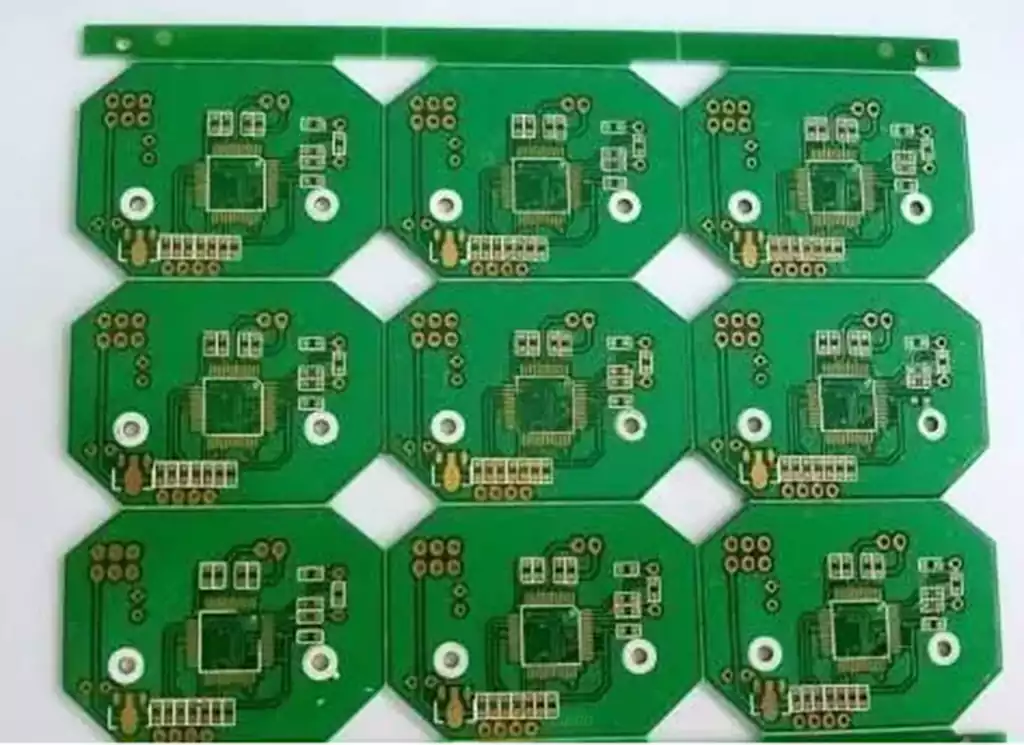
Besides EMI suppression, PCB shielding also provides mechanical protection. After SMT assembly, multiple PCBs are often separated from a production panel. During handling, testing, or transportation, components positioned close to adjacent boards may be susceptible to accidental impact.
A PCB shielding cover creates a protective barrier around sensitive devices, reducing the likelihood of component damage and improving overall product durability.
Thermal Management
PCB shielding can also contribute to heat dissipation. High-power devices such as DSP processors, PMUs, and other power ICs generate considerable heat during operation. Thermal interface materials can be installed inside the PCB shielding can to improve heat transfer.
For applications requiring enhanced cooling performance, nano-carbon thermal coatings or heat-conductive materials may be applied to the PCB shielding cover, helping maintain stable operating temperatures and extending component lifespan.
PCB Shielding Materials
Selecting suitable PCB shielding materials directly affects shielding effectiveness, solderability, manufacturing efficiency, and production cost. The most common materials include nickel silver, stainless steel, and tinplate.
Nickel silver (Cu-Ni-Zn alloy) is the most widely used PCB shielding material because of its excellent solderability and stable SMT performance. Although its EMI shielding capability is slightly lower than stainless steel and its material cost is higher, it offers reliable solder joints and is well suited for automated production.
Stainless steel provides excellent PCB shielding performance and superior mechanical strength at a relatively competitive price. However, it is difficult to solder. Without surface treatment, stainless steel is almost impossible to tin. Even after nickel plating, its solderability still falls short of the reliability required by high-volume SMT manufacturing.
Tinplate offers the lowest PCB shielding performance but features excellent solderability and the lowest material cost. It is commonly selected for products with relatively low EMI shielding requirements.

Types of PCB Shielding
PCB shielding solutions are generally divided into three structural types based on installation and maintenance requirements.
A single-piece PCB shielding can is permanently soldered onto the PCB through SMT assembly. The shielding frame and cover are integrated into one component, providing compact size, excellent PCB shielding performance, and low manufacturing cost.
This design is ideal for consumer electronics that require minimal maintenance after production. For optimal reliability, Cu-7521 nickel silver is commonly selected because of its excellent solderability and resistance to cold solder joints. The PCB shielding cover should include properly designed ventilation openings instead of being completely sealed. Designers should also maintain a minimum height clearance equal to 0.25 mm plus the tallest component, while localized cut-outs may be added where necessary.
A two-piece PCB shielding can, often called a lid-and-frame design, allows the shielding cover to be removed without hot-air rework equipment. This structure greatly simplifies product debugging, testing, and component replacement.
Although more expensive than a single-piece PCB shielding solution, it is widely used in industrial equipment, communication devices, and high-end electronics where maintenance accessibility is important.
PCB Shielding Clip Structure
The PCB shielding clip structure replaces a continuous shielding frame with multiple independent metal clips soldered around the protected circuit area. The PCB shielding cover simply snaps into the clips during assembly.
This PCB shielding solution simplifies installation and maintenance, making it suitable for prototype boards, development platforms, and laboratory testing. However, because of discontinuous grounding and increased board space requirements, its EMI shielding effectiveness is lower than conventional PCB shielding frames. Consequently, this design is rarely used in highly integrated products such as smartphones.
PCB Shielding Design Guidelines
Proper PCB shielding design is essential for achieving reliable EMI protection.
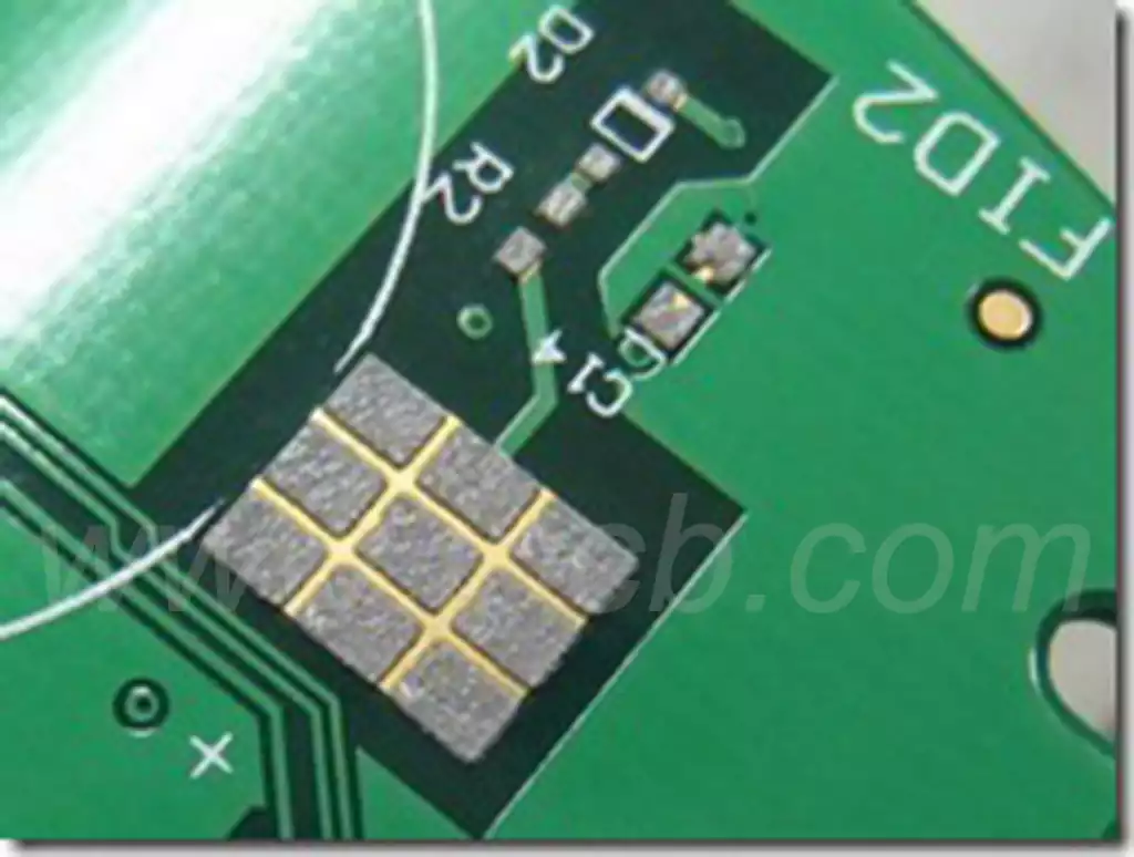
The recommended solder pad width is 0.6–0.8 mm, with a pad length of 3–5 mm and a spacing of 1 mm between adjacent pads. Extended solder tabs matching the pad length improve solder joint strength and structural stability.
Since most PCB shielding cans are installed using SMT equipment, the shielding frame should include a 5 mm diameter vacuum pick-up area for automated placement. In addition, each side of the frame typically includes one or two locking holes with diameters ranging from 0.7 mm to 1 mm for securing the PCB shielding cover. Excessive locking holes should be avoided because they make removal more difficult during maintenance.
For products containing high-power components, it should also include 1 mm ventilation holes to improve airflow and thermal performance.
When Is PCB Shielding Necessary?
Not every electronic product requires. The decision should be based on electrical performance, regulatory requirements, manufacturing cost, and operating environment.
Products requiring CE, FCC, or similar EMC certifications may require PCB shielding to satisfy electromagnetic emission and immunity standards. However, some low-power RF modules can still meet certification requirements without additional shielding.
Manufacturers should also evaluate the added material cost and weight introduced by PCB shielding. While it significantly improves EMC performance, it also increases production expenses.
Mechanical design should also be considered. A PCB shielding can occupies board space and may influence product dimensions or industrial design, especially in compact electronic devices.
Finally, the operating environment is an important factor. Industrial automation equipment, communication systems, automotive electronics, and other products operating in strong electromagnetic environments benefit substantially from robust PCB shielding.
PCB shielding is far more than a simple metal enclosure. It is an integrated engineering solution that combines EMI suppression, mechanical protection, and thermal management. By selecting appropriate materials, choosing the right structure, and following proven design practices, manufacturers can improve product reliability, enhance EMC performance, and achieve an optimal balance between electrical performance, manufacturability, and production cost.