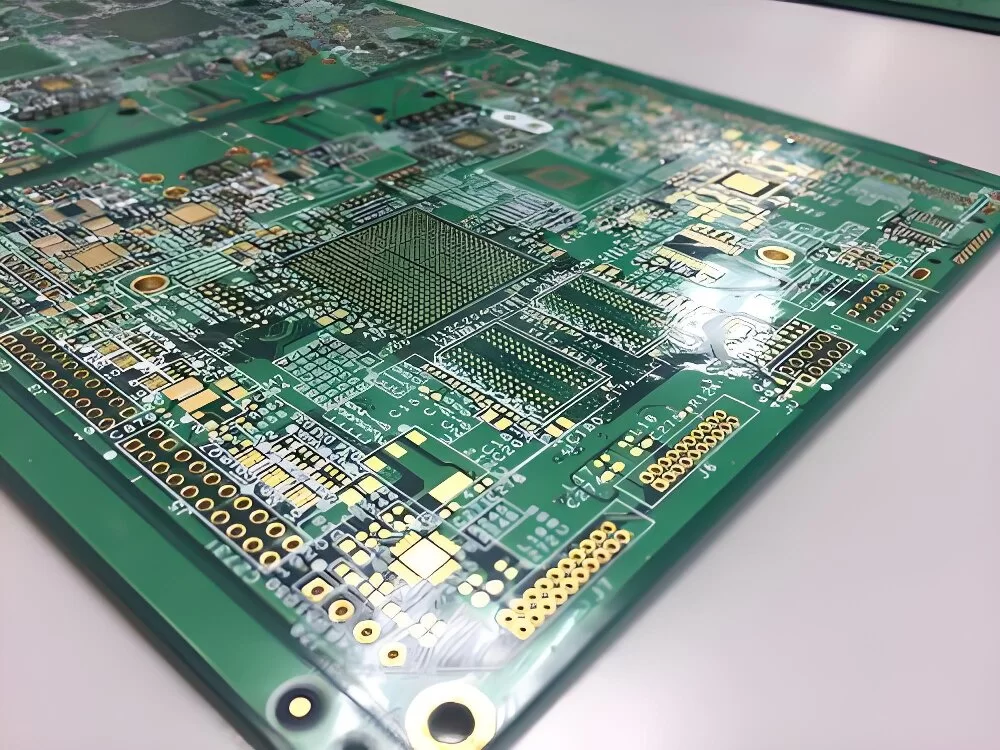
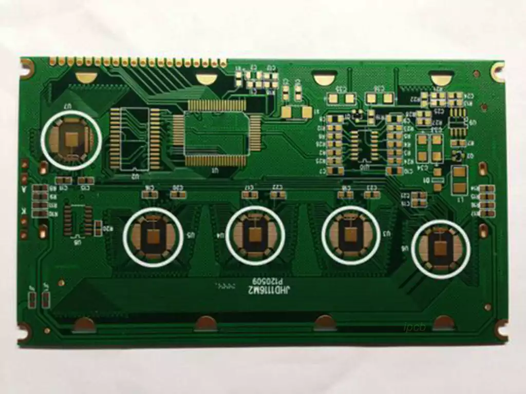
A double sided ceramic PCB, also known as a double-layer ceramic PCB, is one of the most widely used substrate types in modern electronics manufacturing. It serves as a critical foundation for a broad range of consumer, industrial, and high-end electronic products.
From a structural perspective, a single sided ceramic PCB features a conductive circuit layer on only one side of the substrate, limiting routing space and circuit complexity. In contrast, a double sided ceramic PCB incorporates conductive copper circuitry on both sides of the ceramic substrate. Compared with a single-sided design, it provides an additional copper layer, significantly increasing routing capacity and design flexibility.
Among various ceramic PCB configurations, double sided ceramic PCBs offer an excellent balance between performance, manufacturability, and cost. Compared with single-sided ceramic boards, they provide substantially greater routing density and circuit integration. Compared with multilayer ceramic PCBs, they feature a simpler manufacturing process, lower production complexity, and reduced development costs while still delivering excellent electrical and thermal performance. As a result, they have become the preferred solution for most medium- to high-end electronic applications.
Key Advantages of double sided Ceramic PCBs
Flexible Material Selection for Harsh Operating Environments
Applications involving high frequencies, elevated temperatures, corrosive environments, or high-power operation require substrate materials with exceptional performance characteristics. Multilayer ceramic structures are more susceptible to issues such as layer delamination and material mismatch caused by complex lamination processes. double sided ceramic PCBs feature a simpler and more reliable structure, allowing engineers to select specialized ceramic materials optimized for high-frequency, high-temperature, or corrosion-resistant applications. This flexibility enables reliable operation in demanding environments.
Supports Miniaturized Electronic Designs
As electronic products continue to become smaller and lighter, PCB routing density has become increasingly important. By utilizing conductive copper layers on both sides of the substrate, double sided ceramic PCBs provide significantly more routing space than single-sided boards. Circuits that previously required two separate single-sided boards can often be integrated onto a single double sided PCB through optimized component placement and dual-side routing, reducing overall product size without compromising performance.
Excellent Cost-Effectiveness and Stable Manufacturing Yield
Ceramic PCB fabrication requires extremely high machining precision. Multilayer ceramic boards are more likely to experience manufacturing defects such as layer misalignment, interlayer short circuits, and ceramic cracking, which can reduce production yield and increase manufacturing costs.
After years of industrial development, double sided ceramic PCB manufacturing has become highly mature and standardized. The process delivers stable production yields, greater manufacturing tolerance, and lower overall production costs than multilayer ceramic boards, making it a highly cost-effective solution for volume production.
Broad Compatibility Across Electronic Applications
Double sided ceramic PCBs provide a moderate level of circuit integration that satisfies the requirements of most electronic systems. Whether used in standard consumer electronics or sophisticated industrial equipment requiring higher circuit density and precision, they can accommodate a wide range of circuit designs through optimized PCB layout and electrical design.
Functional Layer Separation Improves System Reliability
Modern electronic systems often require a PCB to simultaneously perform signal transmission, power distribution, grounding, electromagnetic shielding, and current return functions.
The double sided structure enables functional layer separation, with one side dedicated primarily to signal routing and component mounting, while the opposite side can serve as a continuous ground plane. This configuration provides a stable reference potential, minimizes electromagnetic interference (EMI), improves power integrity, and enhances overall electrical performance and system reliability, making it particularly suitable for high-performance electronic designs.
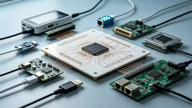
Major Applications of double sided Ceramic PCBs
Consumer Electronics
Double sided ceramic PCBs are widely used in consumer electronic products, including smartphones, portable wireless devices, wearable electronics, smart home appliances, and other intelligent devices. Their excellent thermal performance and long-term reliability help extend product lifespan while reducing failure rates.
Power Electronics
The open double sided structure simplifies component placement, soldering, inspection, and maintenance. These boards are extensively used in LED lighting systems, industrial power supplies, relay control circuits, AC/DC and DC/DC power converters, and other power electronic equipment that requires stable current transmission and continuous high-frequency operation.
Automotive Electronics
Automotive electronic systems must withstand harsh operating conditions, including rapid temperature cycling, vibration, humidity, and long-term mechanical stress. double sided ceramic PCBs provide excellent thermal conductivity, high power-handling capability, and outstanding resistance to aging, making them ideal for automotive LED lighting, body control modules, engine management systems, automotive sensors, and other mission-critical vehicle electronics.
Telecommunications and Networking
With their low dielectric loss, excellent high-frequency characteristics, and strong resistance to electromagnetic interference, double sided ceramic PCBs are widely deployed in routers, network switches, communication base stations, optical communication equipment, and other telecommunications infrastructure, ensuring reliable high-speed signal transmission and precise data processing.
Medical Electronics
Medical devices demand exceptional reliability, accuracy, and long-term operational stability. double sided ceramic PCBs offer outstanding electrical stability and an extremely low failure rate, making them well suited for patient monitoring systems, clinical diagnostic equipment, portable therapeutic devices, intelligent medical instruments, and other precision healthcare applications that require continuous, accurate performance.
Double sided ceramic PCBs achieve an outstanding balance between electrical performance, thermal management, manufacturing maturity, and cost efficiency. Their moderate circuit integration capability, stable production yield, and proven manufacturing technology make them an ideal choice for a wide variety of applications, including consumer electronics, power electronics, automotive systems, telecommunications equipment, and medical devices. As a reliable and economical ceramic substrate solution, double sided ceramic PCBs continue to play a vital role in the development of modern high-performance electronic products.