Heat Sink Design and Microscopic Electroplated Windows in PCB Board Amplifiers
Power amplifiers inevitably experience significant heat loss during the conversion of DC power into AC signals. Whether it’s the low conversion efficiency of linear amplifiers or the on-resistance and switching losses of switching power amplifiers, these factors instantly accumulate into substantial Joule heat on the tiny power transistor chip.
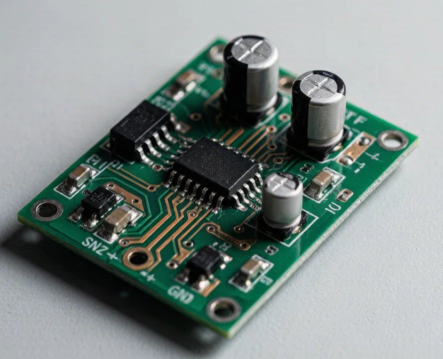
If the PCB board amplifier cannot dissipate this heat within milliseconds, the surge in junction temperature will directly trigger the chip’s thermal shutdown protection, and may even lead to thermal decomposition and structural delamination of the substrate resin.
Microscopic Thermal Via Geometry and Array Distribution
For power transistors using surface mount packages, the bare copper pads of the PCB board amplifier are the first physical barrier for heat diffusion downwards.
Heat conduction within vias primarily relies on the electroplated copper layer on the via walls. According to Fourier’s law of thermal conductivity, thermal resistance is inversely proportional to the thermally conductive cross-sectional area. Excessively large via diameters can cause severe capillary solder wicking during surface mount reflow soldering, drawing away solder intended for the power transistor base and creating large microscopic voids. Conversely, excessively small via diameters lead to plating difficulties and insufficient copper thickness on the via walls.
Therefore, the optimal via diameter for PCB board amplifiers should be strictly controlled at 0.3 mm, with the drill center-to-center spacing between 0.8 mm and 1.0 mm.
To achieve 100% void-free soldering at the bottom of the power transistors, modern high-power PCB board amplifiers must employ a resin-filled via followed by electroplating for smoothing. First, the thermal vias are filled with resin of high thermal conductivity, then a smooth layer of pure copper is electroplated onto the surface. This not only completely eliminates the risk of solder leakage but also imparts extremely high three-dimensional thermal conductivity to the bottom pads.
The thickness of the thermally conductive copper plating and physical windowing for soldering:
In PCB board amplifiers, the thickness of the copper foil directly determines the rate of horizontal heat diffusion.
A standard one-ounce copper layer will cause a significant temperature rise when subjected to continuous power output of 10 amps or more. High-specification PCB board amplifiers must increase the copper thickness of the main power rails and power output layers to two or even three ounces. Heavy copper not only significantly reduces trace resistance but also greatly expands the physical volume of the heat sink.
To significantly increase current carrying capacity without increasing the number of PCB layers, engineers typically create bare copper windows in the high-current, high-power paths of the PCB board amplifier, meaning they are not covered with solder mask. During subsequent wave soldering or manual assembly, a layer of solder alloy with a thickness of 0.5 mm to 1 mm solidifies in the windowed area.
Although the conductivity of solder is lower than that of pure copper, its order-of-magnitude increase in thickness dramatically increases the overall cross-sectional area of the traces, thereby reducing the milliohm-level line resistance to the microohm level and greatly suppressing Joule heating of the traces themselves.
Blocking Backflow Contamination and Noise Floor in PCB Board Amplifiers
In PCB board amplifier design, the success of noise control largely depends on the physical topology of the grounding. Amplifier systems simultaneously contain sensitive small signals at the microvolt level (such as preamplifier audio inputs or weak RF modulation signals) and high-power output signals at tens of volts and several amperes.
If the ground currents of these two signals physically overlap on the PCB board amplifier’s ground plane, the ground potential jumps caused by the strong currents will directly contaminate the small signals, creating a severe AC hum or high-frequency howling noise floor.
Physical Separation of Power Ground, Analog Ground, and Digital Ground
A complete PCB board amplifier layout must be strictly separated into electromagnetic and physical isolation zones:
Analog Ground: Provides an excellent clean reference zero potential for the preamplifier, feedback sampling resistors, bias circuitry, and input filter networks. The area beneath the analog ground must be extremely clean, and no high-frequency switching traces or high-current return flows should pass through it.
Power Ground: Carries the intense charging and discharging currents of the power transistor switching output, speaker load, RF antenna, and large-capacity power supply filter capacitor. Power ground copper plating must be extremely wide and flat to reduce high-frequency inductance.
Digital Ground: Used for the return current of the digital control bus, modulator, and core digital logic.
Star-Topological Single-Point Grounding and Single-Point Bridging Mechanism
In PCB board amplifiers, avoid indiscriminately mixing analog ground and power ground with large areas of copper plating across the entire board. Doing so will cause a strong current of several amperes on the power ground to diffuse along a low-impedance path to the analog ground area, resulting in a significant ground potential shift.
To completely eliminate this contamination path, PCB board amplifiers must enforce star-topological single-point grounding:
Analog ground and power ground can only be physically connected at a single point on the entire board. The optimal physical location for this junction point is directly below the negative pad of the large-capacity power supply filter capacitor, or at the designated analog ground and power ground junction pin of the power amplifier chip.
During layout design, completely separate the analog ground and power ground with ground cutouts. The two regions are connected at a single point via a zero-ohm surface-mount resistor or a high-frequency ferrite bead. The bead exhibits micro-ohm low impedance under DC conditions and high impedance at high frequencies, effectively sealing the intense noise generated by high-frequency switching on the power ground within the power region.
Class D and RF PCB Board Amplifier Loop Minimization
With the continuous increase in switching frequencies of switching power amplifiers and the widespread adoption of gallium nitride-based RF PCB board amplifiers, the voltage and current change rates at switching nodes have reached extremely high levels.
Faced with such intense electromagnetic transients, even a tiny parasitic inductance of one nanohenry or a parasitic capacitance of one picofarad on the trace can cause catastrophic electromagnetic interference and high-frequency ringing in the PCB board amplifier.
Millimeter-Level Squeezing of High-Frequency Transient Current Loops
In switching PCB board amplifiers, the current on the power rail undergoes a rapid jump during the instant the power transistor turns on and off. According to the principle of electromagnetic induction, when a current with an extremely high rate of change passes through the parasitic inductance of a trace, it induces a huge overshoot voltage spike.
If there is a high level of parasitic inductance in the high-frequency decoupling circuit of a PCB board amplifier, the instantaneously generated overshoot voltage spike can directly break down the gate or drain of the power transistor.
To suppress the parasitic inductance to the nanohenry level, the power supply decoupling capacitors in the PCB board amplifier must follow a strict geometric hierarchy layout:
The physical distance between ultra-high frequency surface-mount decoupling capacitors must be millimeter-level, placed directly at the very ends of the power and ground pins of the power chip, and the via path to ground must be minimized.
The closed loop formed by the power pin, decoupling capacitor, and ground pin must have a geometric area on the PCB board amplifier layout of less than ten square millimeters. The smaller the loop area, the weaker the electromagnetic antenna effect of the radiated magnetic field.
Electric Field Radiation Shielding and Parasitic Capacitance Squeezing of Switching Nodes The switching node, connecting the output power transistor and the output low-pass filter inductor, carries a high-frequency, high-voltage square wave signal with an extremely high voltage change rate. In physical space, this node is equivalent to a strong source of electric field radiation.
In PCB board amplifier layout design, the copper plating of the switching node must meet current carrying requirements while compressing its geometric surface area to physical limits; it is strictly forbidden to stretch it into long lines running across the board.
The inner layer immediately below the copper plating of the switching node must maintain a 100% intact ground plane. Through the tight parallel-plate capacitance effect, the electric field lines radiating upwards from the switching node are drawn downwards and attracted to the ground plane, preventing them from applying electric field coupling to surrounding weak signal traces.
Advanced PCB Board Amplifier Physical Layer Engineering Design Red Lines
To ensure that high-power, high-fidelity PCB board amplifiers do not experience excessive noise floor, thermal runaway, or self-oscillation breakdown during prototyping and mass production, the hardware engineering team must enforce the following six physical red lines during design rule checks:
Power Rail and High-Current Trace Current Carrying Capacity Red Lines
For PCB board amplifier power rails and output traces carrying continuous high current, their trace width calculations must be strictly based on the physical limit of 1.5 amps per millimeter of trace width with a 1-ounce copper thickness. At this point, the trace temperature rise can be controlled within 10 degrees Celsius. If a 2-ounce copper thickness is used, this can be relaxed to 2.5 amps per millimeter of trace width.
This prevents the traces from generating severe Joule heating due to excessive copper resistance during continuous full-power output, which could cause the PCB board amplifier substrate resin to fail and debond due to exceeding the glass transition temperature, or even directly burn out the traces.
High-Frequency Transient Decoupling Loop Geometric Area Red Line: The total area of the physical loop formed by the power chip’s power pins, surface-mount decoupling capacitors, and power ground on the PCB board amplifier layout must be strictly controlled within a 10 square millimeter limit.
This suppresses parasitic inductance of the traces to below 0.5 nanohenries, eliminates ultra-high voltage spikes generated by high-frequency switching transients, and prevents the power transistor from being overvoltage-damped and burned out.
Power Transistor Thermal Via Density and Resin-Plug Specifications: Thermal vias located directly below the power transistor’s heatsink base must have a drill diameter of 0.3 millimeters and a hole spacing of less than or equal to 0.9 millimeters. Furthermore, a resin-plugging and plating smoothing process must be mandated during the PCB board amplifier manufacturing stage.
This completely eliminates the capillary loss of solder from the bottom of the power transistor along the hollow thermal vias during surface-mount reflow soldering, preventing large solder joint voids and thermal blocking layers on the chip bottom.
Small-Signal High-Impedance Feedback Loop Protection Red Line: The voltage divider network connecting the output terminal and the feedback pin of the main control chip must be placed directly against the chip’s feedback pin. Feedback-sensitive traces must be 100% grounded on both the inner and outer layers of the PCB board amplifier, and must never cross below switching nodes or high-frequency power inductors in parallel.
This prevents the high-level switching electric field from directly coupling into the sensitive feedback loop, which could inject difficult-to-eliminate out-of-band noise into the PCB board amplifier output, or even cause a collapse in the system phase margin, leading to high-frequency self-oscillation.
Single-Point Connection Red Line for Analog Ground and Power Ground: Analog ground and power ground are only allowed to be connected at a single point on the entire PCB board amplifier via a zero-ohm resistor or ferrite bead at the negative pad of the main power filter capacitor. The width of the gap between the two ground planes must be greater than or equal to 0.5 mm.
This completely cuts off the physical path for high-current power backflow into the weak analog preamplifier ground, eliminating output background noise, hum, and distortion caused by ground potential jumps.
Power Output Low-Pass Filter Inductor Magnetic Field Coupling Protection
For low-pass filters at the output of switching PCB board amplifiers, the power inductors for both channels (e.g., left and right channels, or differential output) must be physically positioned at a 90-degree angle, or maintain a physical distance of at least 1.5 times the inductor body height.
This prevents strong mutual inductance magnetic field coupling between high-current, high-frequency inductors, eliminating crosstalk between channels and excessive out-of-band harmonic secondary radiation.