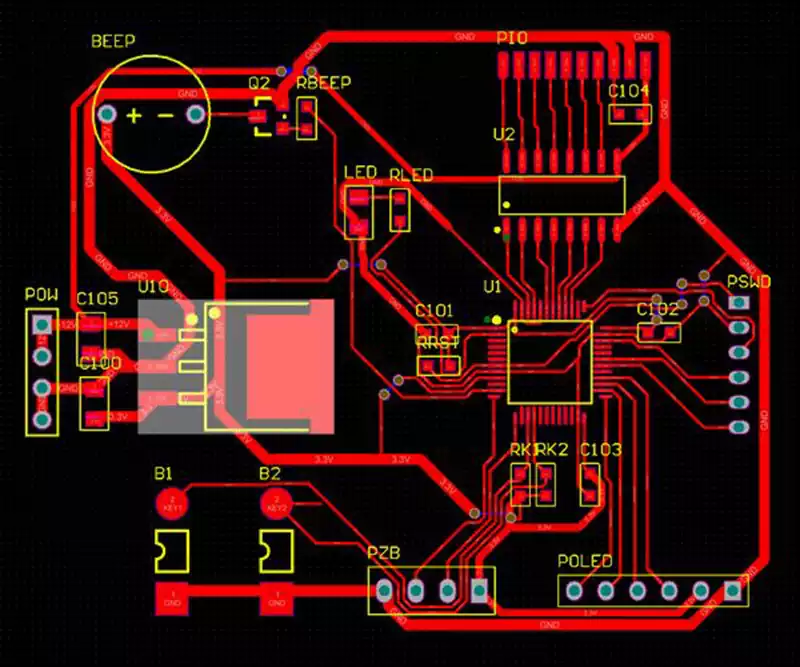
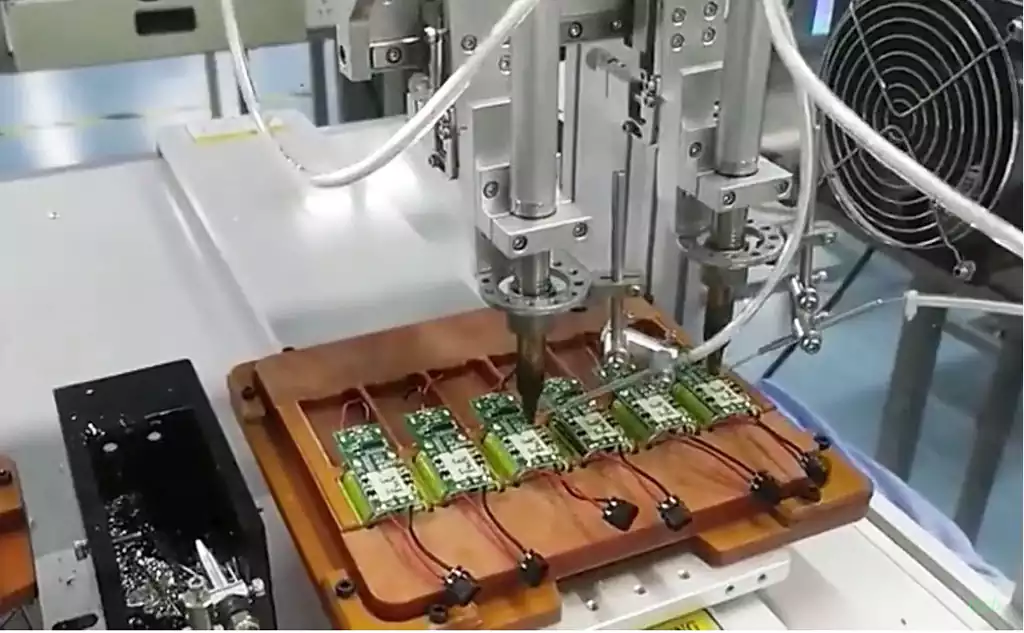
In the hardware design and mechanical engineering of printed circuit boards (PCBs), mounting pcb holes, seemingly just ordinary round holes on the board, are crucial hubs connecting the electrical and physical worlds. A well-designed mounting hole pcb not only fulfills the physical function of securely fixing the PCB to the device casing or base, but also profoundly affects the overall mechanical stress distribution, electromagnetic compatibility (EMC) performance, electrostatic discharge (ESD) protection pathways, and the reliability of production and assembly.
A deep analysis of the technical details of PCB mounting holes helps to fully understand their classification characteristics, design specifications, stress control, electrical safety, and manufacturing processes.
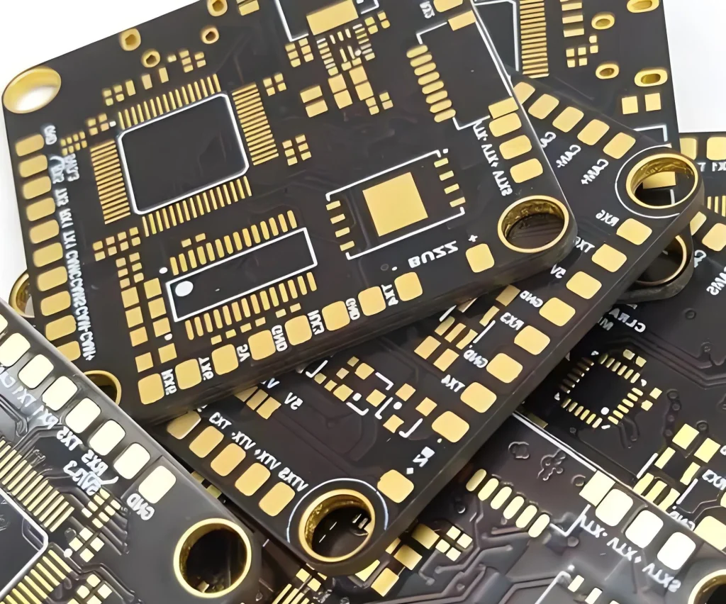
Basic Physical Definition and System Functions of Mounting Holes
PCB mounting holes are through holes or grooves machined at specific locations on the substrate during PCB manufacturing through mechanical drilling or CNC milling processes for fastening, positioning, or support. From a systems engineering perspective, mounting holes have three core functions.
First is physical support and mechanical positioning. Electronic products are subjected to mechanical stress from various directions during transportation, drops, vibrations, and daily use. Mounting holes, secured to the device cavity using fasteners such as screws, nuts, copper pillars, or plastic clips, restrict the board’s displacement and deformation in three-dimensional space, preventing surface mount device (SMD) solder joint cracking or pin breakage due to board bending stress.
Secondly, mounting holes serve for electrical connections and system grounding. In many metal-cased or shielded electronic devices, copper-plated mounting holes are the physical interface connecting the PCB signal ground or safety ground to the system’s metal casing (chassis ground). With proper grounding design, mounting holes can provide a low-impedance return path for high-frequency noise and form an optimal discharge channel for electrostatic discharge.
Finally, mounting holes facilitate structural alignment and assembly tolerance absorption. In multi-board stacking or precision module assembly, mounting holes, along with positioning holes, ensure precise alignment between connectors, buttons, displays, and interface devices (such as USB and HDMI) and casing openings, absorbing cumulative deviations caused by board manufacturing tolerances and casing machining tolerances.
Classification and Essential Differences: Non-Copper Holes vs. Copper Holes
From the perspective of PCB manufacturing processes and electrical characteristics, mounting holes are mainly divided into two categories: non-copper-plated mounting holes (NPTH) and copper-plated mounting holes (PTH). The choice of which type of mounting hole to use depends on specific circuit isolation requirements, structural materials, and grounding strategies.
Non-Copper-Plated Mounting Holes (NPTH) Non-copper-plated mounting holes have exposed walls on insulating substrates such as FR-4, with no copper layer inside.
In terms of manufacturing processes, non-copper-plated holes are typically manufactured after dry film curing, etching, and solder mask printing, using a secondary drilling process (forming a shaped hole) or contour milling. Because the hole walls have no copper, they are electrically completely insulated from all conductive layers inside the PCB.
Applications of non-copper-plated holes typically include:
First, areas requiring high electrical isolation. For example, the boundary between high and low voltage circuits, and the edge fixing points of high-voltage power boards, where it is essential to prevent any risk of electrical breakdown between screws and internal traces.
Second, in scenarios where purely mechanical fixing is used with plastic studs or spacers, electrical grounding is not required.
Third, it prevents metal screws from excessively tightening and breaking the copper layer, causing tiny copper shavings to fall onto the high-density board surface and cause short circuits.
Copper-plated mounting holes (PTHs) have walls thickened through chemical copper plating and electroplating, forming a complete copper tube structure, and typically have metal pads on both the top and bottom of the hole opening.
During manufacturing, copper-plated mounting holes are processed simultaneously with ordinary electrical vias and plug-in lead holes (PTH holes). After drilling, they undergo copper plating and board surface electroplating, resulting in a copper layer of a specific thickness (usually above 20 micrometers) on the hole walls.
The core advantages of copper-plated mounting holes are their low impedance conductivity and higher mechanical strength. Copper-plated holes can be directly connected to the PCB’s ground plane through inner or surface copper foil. When the metal screw is screwed in and presses against the pad, an extremely low impedance metal contact can be established. Furthermore, the copper layer on the hole walls significantly enhances their mechanical rigidity under pressure, enabling them to withstand greater tensile and shear stresses than non-copper-plated holes.
Irregularly Shaped Holes and Mounting Slots
In addition to standard circular mounting holes, certain specialized mechanical structures utilize rectangular, elliptical, or arc-shaped mounting slots. These irregularly shaped slots are primarily used to absorb thermal expansion stress or address installation tolerances.
When PCBs operate in high-power environments or outdoor environments with drastic temperature variations, there is a difference in the coefficients of thermal expansion between the PCB substrate (e.g., FR-4) and the metal casing. If all mounting points are rigid circular holes, the enormous internal stress generated by thermal expansion and contraction can cause severe warping of the circuit board or even breakage of internal traces. A structure using a circular hole on one side and a long, narrow mounting slot on the other allows for a small thermal displacement along a specific axis, thereby releasing thermal stress.
Mechanical Stress Analysis and Physical Design Specifications
Screw tightening is a process of converting rotational torque into axial preload. When a screw is tightened into a PCB mounting hole, the fastener head and nut apply significant local compressive stress to the PCB material. If poorly designed, this stress can become a fatal hidden danger for PCB failure.
Torque and Substrate Stress Mechanism
The main materials of PCBs (such as FR-4 fiberglass epoxy composite) have good tensile strength, but their local compressive and shear strength are limited. When the torque applied by the fastening screw exceeds the material’s bearing capacity limit, the screw head will directly crush the solder mask and copper foil on the PCB surface, and may even cause the internal fiberglass layer to crack. This phenomenon is called substrate crushing or delamination.
To prevent stress concentration, the design of mounting holes must strictly control the contact area of the screw head or metal washer. By increasing the contact area, the pressure per unit area can be significantly reduced.
The Role and Anti-Loosening Mechanism of Washers
Using washers around mounting holes is an effective way to distribute mechanical stress and prevent screw loosening. Common types of washers and their physical functions are as follows:
Flat Washers are mainly used to increase the bearing area, evenly distributing the concentrated load of the screw head to a larger pad area, protecting the solder mask from wear.
Spring washers and too-lock washers utilize elastic deformation to maintain continuous axial tension, preventing screw loosening in long-term vibration environments.
For copper-plated mounting holes, serrated too-lock washers can pierce the oxide layer or residual solder mask on the copper pad surface when tightened, establishing a more robust metal-to-metal electrical contact, which is particularly important for high-frequency grounding and electrostatic discharge.
Keepout Zone Design
To ensure absolute safety of mounting holes during assembly and use, layout engineers must define strict physical and electrical keepout zones for each mounting hole in PCB design software. Keepout zones typically consist of three layers:
The first layer is the keepout zone for screw heads and installation tools (such as screwdriver sockets and electric screwdriver bits). This area must not only accommodate the physical outer diameter of the screw head but also allow for mechanical tolerances that may arise during high-speed rotation of the assembly tool. No surface-mount components, test points, or traces should be placed within this area.
The second layer is the solder mask keepout zone. Covering areas directly pressed by screw heads or washers with solder resist ink is not recommended. Solder resist ink is a brittle resin material that is highly susceptible to cracking and peeling under high pressure and torque. Peeling ink fragments can contaminate surrounding precision components, and residual ink, after being cooled under pressure, can cause a decrease in screw preload, leading to loosening. Therefore, the fastening contact surfaces around mounting holes should be designed as bare copper pads or fully open.
The third layer is the clearance zone for inner layer traces and vias. Because screw tightening creates a radial stress diffusion field around mounting holes, if inner layer traces or electrical vias are too close to the edge of the mounting hole, mechanical stress can cause micro-cracks in the inner layer copper foil or breakage of the via copper walls. It is generally required that all inner layer traces and unrelated vias maintain a safety distance of at least one millimeter from the edge of the mounting hole.
Electrical Design and System-Level EMC/ESD Strategy
Mounting holes are not only mechanically fixed components but also critical nodes in system-level electromagnetic compatibility (EMC) and electrostatic discharge (ESD) protection design. Properly designing the electrical connections of mounting holes can significantly improve the circuit board’s anti-interference capability and reduce external radiation.
Topological Relationship between Chassis Ground and Signal Ground
In complex electronic systems, multiple ground planes often exist, the most typical being the system circuit’s signal ground (GND) and the device’s metal chassis ground (PGND/CHASSIS). Mounting holes are often the meeting points of these two types of ground planes.
The direct connection strategy involves directly connecting the copper-plated mounting holes to the inner or surface signal ground plane. This strategy is suitable for low-frequency systems or devices with well-shielded metal housings, providing the lowest possible grounding impedance. However, in environments with high-frequency common-mode interference or ground loops, direct connections can cause high-frequency noise from the chassis to backflow into the signal ground through the mounting holes, leading to abnormal circuit operation.
The isolation connection strategy completely disconnects the copper foil around the mounting holes from the signal ground, maintaining mechanical fixation only through non-copper-plated holes or isolated copper-plated holes. This method breaks the ground loop, but leaves the PCB without an effective electrostatic discharge path. Accumulated static charge may find weak points on the board and cause electrical breakdown.
The hybrid impedance connection strategy is currently the most commonly used solution in mid-to-high frequency and complex systems. This involves connecting the mounting hole pads to the housing ground, but the housing ground and signal ground are not directly connected. Instead, they are bridged by parallel high-voltage capacitors, zero-ohm resistors, or ferrite beads. The capacitors exhibit high impedance in the DC and low-frequency ranges, successfully isolating the low-frequency ground loop and DC ground potential difference; while in high-frequency and electrostatic discharge transients, they exhibit low impedance, providing a fast discharge path for high-frequency interference and high-voltage static electricity.
Via Star/Flower Pattern Array Design
In high-performance PCB design, a ring of small copper-plated vias arranged in a circular pattern is often seen around copper-plated mounting holes. This structure is called a Via Array around Mounting Hole.
The via design incorporates profound electromagnetic and mechanical considerations:
From an electromagnetic perspective, while a single large-diameter mounting hole has copper walls, its high-frequency impedance is relatively high due to the single path. By densely arranging a ring of micro-vias connecting each ground layer around the mounting hole, it’s equivalent to paralleling dozens of low-inductance paths, significantly reducing grounding impedance at high frequencies. This via array forms a physical barrier similar to a Faraday cage, effectively blocking high-frequency electromagnetic waves from radiating outwards along the hole edges or intruding from the outside.
From an electrostatic discharge (ESD) protection perspective, when external high-voltage static electricity is driven into the mounting hole through a screw, the via array can quickly and evenly distribute the transient high current to each ground layer, preventing high-voltage arcs from concentrating on a single path and causing localized high-voltage rebound, thus protecting sensitive internal chips.
From a manufacturing and mechanical perspective, the via structure establishes a multi-point supported three-dimensional “anchoring” structure between the metal pads and the PCB substrate, greatly enhancing the mounting hole pads’ resistance to tearing and peeling.
Creepage & Clearance
In PCB design involving high-voltage power electronics, switching power supplies, or medical electronic equipment, the safe clearance of mounting holes must strictly adhere to relevant international safety standards (such as IEC 60950, IEC 62368, etc.).
Clearance refers to the shortest spatial distance between two conductive components in air; creepage distance refers to the shortest distance measured along the surface of an insulating material between two conductive components.
Because metal screws are good conductors, after being screwed into a mounting hole, the screw head and stud effectively become an extended electrode around the high-voltage circuit. If the mounting hole is too close to a high-voltage trace or high-voltage component, high-voltage current may break down the air along the solder mask layer on the PCB surface, discharging to the screw and metal casing, causing serious safety accidents or equipment damage.
Therefore, mounting holes near high-voltage areas must have sufficient creepage distance, and when necessary, the creepage distance can be artificially increased by milling isolation slots between the mounting hole and the high-voltage trace to cut off the surface discharge path.
Manufacturing Process and Assembly Details
The quality of PCB mounting holes depends not only on the layout and routing during the design phase but also on the actual manufacturing process in the PCB factory and subsequent SMT assembly and depaneling processes.
Drilling and Milling Process Accuracy
Mounting holes are typically machined using high-speed CNC drilling machines during the PCB manufacturing drilling stage. Because mounting holes are generally larger than ordinary electrical signal vias, the drill bit generates greater mechanical impact and heat when cutting the substrate.
Drilling accuracy is constrained by various factors. The wear of the drill bit directly affects the roughness of the hole wall. If the drill bit is severely worn, it can cause tearing of the glass fibers inside the FR-4 substrate during cutting, producing tiny burrs and voids. These voids easily absorb plating waste liquid during subsequent copper plating processes, leading to internal ion migration and decreased insulation.
Furthermore, the eccentricity tolerance of the CNC spindle can cause hole misalignment. If the mounting hole position misalignment exceeds the design tolerance, the entire board will experience screw misalignment and forced insertion, resulting in huge assembly shear stress when assembled into the metal casing.
Solder Mask Opening Strategies
The solder mask treatment strategy for mounting hole pads directly affects assembly reliability and surface coating durability.
Full Opening: Full opening means the metal pads on both sides of the mounting hole are completely exposed above the copper layer (or gold plating, tin plating), with the solder mask ink receding beyond the outer edge of the pads. This strategy is most beneficial for establishing good electrical contact and physical clamping between screws and washers.
Partial Opening (or Half Opening): Copper is exposed only in the annular area of screw contact, while solder mask is retained around the pads. This method is often used in applications where the exposed copper foil area needs to be limited to prevent corrosion.
Tented Hole: Solder mask ink completely covers the mounting hole and its pads. This treatment is only suitable for non-copper-plated holes or purely structural holes that do not require electrical grounding. If copper-plated grounding holes are fully covered with solder mask ink, the solder mask ink will easily tear when the screw is screwed in, causing ink fragments to become trapped between the screw and the copper layer. This not only fails to guarantee reliable mechanical fastening but also disrupts the grounding path.
Panelization and Depaneling Stress
In mass industrial production, individual PCBs are typically assembled into panels for SMT (Surface Mount Technology) assembly and wave soldering. After production, the individual PCBs are separated from the panels using V-cuts or milling stamp holes.
If mounting holes are too close to the depanel edge or stamp holes, strong tearing stress will propagate along the board to the area around the mounting holes during mechanical cutting or manual breakage. If sensitive components or inner layer traces are located near the mounting holes, depaneling stress can easily cause inner layer trace breakage or microcracks in MLCCs (Multi-Layer Ceramic Capacitors).
Therefore, standards require sufficient safety buffer distance between mounting holes and the depanel edge, and rigid support must be provided for the mounting hole area in the depanel fixture design.
Common Engineering Defects, Failure Modes, and Reliability Analysis
Throughout the product lifecycle, failures caused by improper mounting hole design or uncontrolled assembly processes are common. In-depth analysis of these failure modes is crucial for improving product reliability.
Substrate Micro-cracks and Circuit Breakage Caused by Overtightening of Screws
This is the most common form of mechanical failure. If production line workers or automated electric screwdrivers set the torque too high, exceeding the allowable stress of the PCB material, the screw head pressing against the solder pads can cause internal delamination and micro-cracks in the FR-4 substrate around the mounting holes.
These micro-cracks may not immediately manifest as electrical faults during factory testing. However, as the product experiences power-on/off thermal cycling and ambient temperature fluctuations at the user end, the thermal expansion mismatch between the substrate and copper foil causes the micro-cracks to gradually propagate, eventually breaking the fine inner layer traces that traverse the area, resulting in intermittent product malfunctions or permanent open circuits.
Electrical Short Circuits Caused by Cutting Debris
When self-tapping screws or machine screws are forcibly tightened into non-copper-plated mounting holes or unopened solder mask surfaces, the screw threads forcibly cut into the PCB substrate and solder mask layer, generating tiny resin dust and solder mask debris.
If there are dense, unexposed copper traces or high-density SMT components around the mounting holes, these tiny debris particles can travel across the board surface due to equipment vibration. More seriously, if the metal layer on the copper-plated holes is scraped off, the resulting metal fragments can easily fall under the pins of fine-pitch chips (such as QFN and BGA), causing irreversible short circuits and burnout of adjacent pins.
Electrochemical Migration and Galvanic Corrosion: When copper-plated mounting holes are in direct contact with screws, and the equipment operates in harsh environments such as humid conditions or salt spray, the potential difference between different metals can trigger electrochemical corrosion.
For example, there is a different standard electrode potential between the solder mask coating (such as tin, gold, or organic solderability protectant) on the surface of the copper-plated hole and the steel, stainless steel, or galvanized screws. In the presence of moisture and trace amounts of salt acting as an electrolyte, the metal with the lower potential will act as the anode and be corroded more rapidly, forming metal oxides and salts. This corrosion not only destroys the low impedance characteristics of grounding, but the resulting corrosion products also spread to the surrounding area, causing a significant decrease in the insulation resistance of adjacent circuits and even triggering electrochemical ion migration (ECM) short circuits.
Interdisciplinary Collaboration and Best Design Practices
Designing PCB mounting holes is not a task that a PCB layout engineer can complete alone; it must be the result of high-level collaboration among multiple disciplines, including Electrical Engineering (EE), Structural Engineering (ME), and Manufacturing Engineering (PE).
3D Model Synchronization and 3D Interference Check
In modern Electronic Design Automation (EDA) tools, a highly integrated MCAD-ECAD collaborative design process has become the standard.
Structural engineers create geometric models of the device housing, structural supports, and studs in 3D CAD software (such as SolidWorks, Creo, etc.) and export the board outline file, containing precise coordinates of the mounting holes, in STEP or IDF format for the PCB engineer.
The PCB engineer imports the coordinates into the EDA software and precisely places the mounting holes and their reserved areas at the corresponding locations. After routing is completed, PCB engineers export a full 3D model of the board, including all electronic components, mounting holes, and screw heads, back to the structural software for comprehensive 3D interference checks. This process fundamentally eliminates basic errors such as mounting hole misalignment and spatial collisions between screw heads and nearby tall components (e.g., electrolytic capacitors, inductors).
Modular and Standardized Hole Layout
To improve product upgradeability and versatility, the layout of PCB mounting holes should adhere as closely as possible to industry standards or internal modular specifications.
In the computer and server industry, standards such as ATX, Micro-ATX, and Mini-ITX define extremely strict requirements for the location, diameter, and grounding pad size of mounting holes, ensuring perfect compatibility between motherboards from different manufacturers and standard chassis.
In embedded and IoT devices, standardized hole layouts enable stacking and reuse between motherboards and different expansion modules, significantly shortening new product development cycles and reducing mold development costs.
Comprehensive Design Checklist Based on the above technical requirements, a systematic evaluation and inspection of mounting holes should be conducted before PCB design archiving and production:
First, confirm that the mounting hole type (PTH or NPTH) fully complies with the system’s grounding strategy and insulation requirements.
Second, confirm that the mounting hole diameter includes copper plating tolerances, and that the finished hole diameter can smoothly pass through screws of the specified size (e.g., M2, M2.5, M3, etc.).
Third, confirm that sufficient keep-away zones have been defined around all mounting holes, with no sensitive components or test points on the surface, no irrelevant traces or vias on the inner layers, and that the keep-away zone covers the screw head and the outer diameter of the mounting tool.
Fourth, confirm that copper-plated mounting holes requiring grounding use appropriate pad openings and via arrays, and that no solder mask is applied.
Fifth, for mounting holes near high-voltage areas, confirm that the creepage distance and clearance from the screw head to the high-voltage trace meet safety certification standards.
Sixth, complete a two-way comparison of the 3D model with the structural engineer to confirm that there is no physical interference in three-dimensional space.
By deeply understanding the mechanical, electromagnetic, and materials science principles behind PCB mounting holes and strictly implementing standardized design processes, engineers can significantly improve the structural robustness, electromagnetic compatibility, and long-term production reliability of hardware products, laying a solid physical foundation for the stable operation of the entire electronic system.