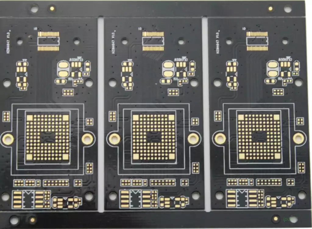
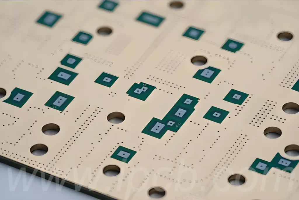
In industrial applications, ceramic substrates are not limited to electronic packaging structures—they are also widely used as insulation and mechanical support components. Therefore, substrate thickness is not a parameter that can be arbitrarily defined. Whether for ceramic materials such as alumina (Al₂O₃) and aluminum nitride (AlN), or for metallization systems such as DBC, DPC, and AMB, substrate thickness directly impacts structural reliability, heat dissipation capability, and subsequent processing stability.
The common ceramic substrate thicknesses available on the market are typically engineering standard thickness ranges that have been gradually established over years of engineering application, taking into account manufacturability, reliability, and processing stability.
Why Can’t Ceramic Substrate Thickness Be Customized Arbitrarily?
Ceramic materials are inherently hard yet brittle, making them highly sensitive to thickness during processing and application.
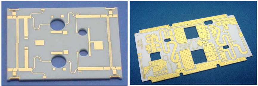
Thickness design is typically influenced by factors such as mechanical strength and flexural strength, thermal conductivity and heat dissipation path design, electrical insulation distance requirements, stress matching with metallization or packaging structures, processing limitations and yield control, and dimensional matching with terminal assembly structures.
In practical applications, unreasonable thickness design can lead to serious consequences. If the substrate is too thin, the risk of cracking and warpage increases, and processing yield drops significantly. If it is too thick, thermal resistance rises, heat dissipation efficiency decreases, and processing costs escalate. Non-standard thicknesses may introduce instability in dicing, metallization, and subsequent packaging processes.
Additionally, in DBC (Direct Bonded Copper) and DPC (Direct Plated Copper) processes, ceramic substrates must withstand the thermal stress from the copper layer, so thickness selection must simultaneously consider structural stability and thermal matching. For these reasons, ceramic substrate thicknesses in industrial production generally converge within a few stable engineering specification ranges.
How Different Application Systems Influence Substrate Thickness
For electronic packaging and power modules, the primary applications include metallized ceramic structures such as DBC, DPC, and AMB systems used in power electronics and semiconductor modules. Ceramic substrates in these structures typically need to simultaneously provide electrical insulation, metal layer support, thermal cycle stress management, and structural support. In engineering practice, thickness must balance strength and thermal performance—making stable standard specifications the preferred approach.
Beyond electronic packaging, ceramic materials are also widely used in non-metallized applications. These include insulating structural components for semiconductor equipment, high-temperature support and positioning parts, components for vacuum and plasma environments, high-voltage insulation isolation components, and precision mechanical support structures. In these applications, ceramics are typically not used as conductive substrates but directly as structural materials to withstand mechanical or environmental loads. Here, thickness primarily serves to meet rigidity, stability, and insulation distance requirements.
Thickness Distribution of Ceramic Substrates in Industrial Applications
From an engineering perspective, ceramic materials can span a wide thickness range across different applications. However, in actual volume production and industrial supply, thickness tends to converge within stable engineering ranges.
For thin precision structures in the 0.25–0.5 mm range, these are primarily used for lightweight and highly integrated applications such as high-frequency electronic devices, miniaturized packages, and certain specialized pre-packaged precision components. Due to the thinner profile, requirements for material consistency, processing precision, and shipping protection are typically higher.
The mainstream industrial engineering thickness range of 0.5–0.635 mm is one of the most widely used engineering thickness ranges, commonly found in power electronics packaging, industrial electronics, and sensor structures. Among these, 0.5 mm and 0.635 mm are well-established standard specifications that offer a good balance between structural stability and processing efficiency.
For high-strength, high-reliability applications around 1.0 mm, this thickness range is typically used in applications requiring higher structural stability, such as power modules and high-reliability industrial equipment. Compared to thinner structures, it offers greater mechanical strength and thermal stability, with a higher likelihood of maintaining structural integrity under long-term operational conditions.
For reinforced and special engineering structures in the 1.2–1.5 mm range, these are primarily used in specialized environmental equipment, heavy-duty structures, and certain custom industrial applications. Greater thickness provides higher rigidity and impact resistance, but also impacts processing costs and heat dissipation paths.
Ceramic Substrate Material Options from iPCB
To meet the varying requirements of insulation performance, thermal conductivity, and structural strength across different applications, iPCB offers a wide range of ceramic substrate products in multiple material types, sizes, thicknesses, and surface roughness specifications—suitable for electronic packaging, industrial insulation, and high-temperature structural applications.
Size, thickness, and surface roughness can all be customized upon request.
If you need further assistance with material selection, dimensional processing, or special structural requirements, please feel free to contact the iPCB team for additional technical support and product information.