The PCB stackup is the foundation of circuit board design, and its configuration directly determines the electromagnetic compatibility (EMC) performance of the entire electronic system. Stackup design is a highly systematic engineering task that requires strict logic and careful planning. In practical product development, designers do not need to build a stackup from scratch through repeated calculations and simulations. Instead, they can leverage proven industry best practices and select an appropriate stackup based on the hardware requirements of the product. This approach significantly improves design efficiency while minimizing common design risks.
Core Principles of PCB Stackup Design
1.Signal Layer Shielding
Every signal layer should be placed adjacent to an internal power plane or ground plane. The large copper area of the reference plane acts as a natural electromagnetic shield, reducing external interference and ensuring signal integrity.
2.Tight Coupling Between Power and Ground Planes
Power and ground planes should be closely coupled by minimizing the dielectric thickness between them. A smaller spacing reduces power loop impedance, enhances plane coupling, and improves power integrity.
3.Shielding for High-Speed Signals
High-speed signals should be routed on internal signal layers sandwiched between two reference planes. The copper planes above and below the signal layer create a closed electromagnetic shielding structure that confines electromagnetic radiation within the PCB while protecting the signals from external interference.
4.Crosstalk Suppression
Adjacent signal layers should be avoided whenever possible because they are prone to electromagnetic coupling and signal crosstalk, which may lead to logic errors or functional failures. If adjacent signal layers cannot be avoided due to layout constraints, a ground plane should be inserted between them to provide effective electromagnetic isolation.
5.Ground Impedance Optimization
Using multiple independent ground planes effectively reduces overall ground impedance. Dedicated ground planes for different functional signal groups help suppress common-mode noise and improve the board’s electromagnetic immunity.
6.Symmetrical Stackup Structure
The overall stackup should remain symmetrical to prevent PCB warpage or deformation during manufacturing, SMT assembly, and operation under varying temperature conditions, thereby improving both manufacturability and long-term reliability.
Recommended PCB Stackup Configurations
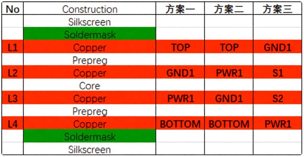
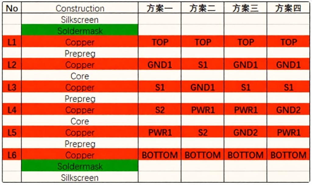
4-Layer PCB Stackup
A standard 4-layer PCB typically has a board thickness of 1.6 mm (62 mil). Under this configuration, the spacing between layers is relatively large, resulting in several limitations. It is difficult to achieve precise impedance control, effective plane coupling, and sufficient electromagnetic shielding. In addition, the large separation between the power and ground planes reduces the board capacitance and weakens noise suppression. Therefore, conventional 4-layer boards are generally suitable only for low-speed, low-precision applications with modest EMC requirements.
Three common stackup configurations are widely used.
Configuration 1 (Recommended)
This configuration is ideal for PCBs with a high component density on the top layer. A continuous ground plane is placed directly beneath the top layer, making the adjacent signal layer the preferred routing layer for critical signals.
This arrangement provides excellent signal integrity (SI). Although its EMI performance is moderate, careful routing practices and EMC optimization techniques can effectively compensate for this limitation. Positioning the ground plane directly beneath the most densely routed signal layer efficiently absorbs and suppresses electromagnetic radiation.
Configuration 2 (Alternative)
This configuration follows essentially the same design philosophy as Configuration 1 and serves as a practical alternative for similar applications.
Configuration 3 (Alternative)
This configuration is mainly intended for through-hole PCB designs. The power plane is placed on the second routing layer, while the bottom layer is assigned as a continuous ground plane to form a closed shielding structure suitable for conventional through-hole assemblies.
Recommendation: Configuration 1 is the preferred choice, while Configurations 2 and 3 are suitable alternatives depending on component placement and routing requirements.
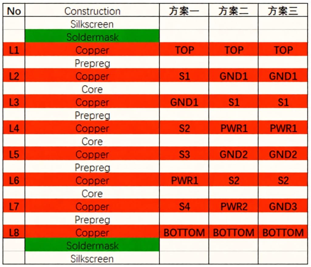
6-Layer PCB Stackup
For designs with highly integrated ICs, high operating frequencies, or stringent EMC requirements, a 6-layer or higher stackup is recommended instead of a conventional 4-layer design.
Four mainstream configurations are commonly used.
Configuration 1 (Alternative)
Suitable for designs requiring extensive routing while maintaining a low manufacturing cost. Because the spacing between the power and ground planes is relatively large, power noise suppression and EMI performance are less effective.
The third layer serves as the preferred routing layer, while routing on the third and fourth layers should be arranged orthogonally to minimize interlayer crosstalk.
Configuration 2 (Alternative)
This configuration places the power and ground planes adjacent to each other, significantly shortening the power return path. It offers excellent electromagnetic absorption, strong EMC performance, and precise impedance control for signal layers, making it suitable for most high-performance digital circuits.
Configuration 3 (Recommended)
This is generally regarded as the optimal 6-layer stackup.
Every signal layer is adjacent to a ground plane, while the power and ground planes are tightly coupled. Controlled impedance can be achieved across all routing layers. The dual ground planes effectively absorb magnetic fields and provide continuous, low-impedance return paths for all signal traces, provided that the power and ground planes remain uninterrupted.
This configuration delivers outstanding signal integrity, power integrity, and EMC performance. Its only drawback is the reduced number of available routing layers, which requires more advanced PCB layout planning.
For optimal performance, the dielectric thickness between Layers 4 and 5 should be minimized. Layer 3 should be used as the primary routing layer for high-speed and EMI-sensitive signals.
Configuration 4 (Alternative)
This configuration is similar to Configuration 3, except that the power plane and ground plane are interchanged.
If the bottom layer contains densely populated components, using the power plane as the signal reference may increase crosstalk and power noise. Configuration 3 generally provides superior performance because bottom-layer signals reference a ground plane, resulting in shorter return paths and improved signal and power integrity.
Recommendation: Configuration 3 is the preferred solution, while Configurations 1 and 2 are suitable alternatives.
8-Layer PCB Stackup
An 8-layer PCB provides greater flexibility for implementing effective shielding structures and return paths, making it well suited for medium- to high-end high-speed electronic products.
Four mainstream configurations are commonly adopted.
Configuration 1 (Alternative)
Suitable only for applications with relatively low power integrity and EMC requirements. Because it contains fewer ground planes, its shielding capability and electromagnetic suppression performance are relatively limited.
Configuration 2 (Alternative)
This configuration is derived from the optimal 8-layer stackup and incorporates additional reference ground planes to improve EMI performance while maintaining accurate impedance control. It is particularly suitable for multi-power-rail systems.
Configuration 3 (Recommended)
This is widely regarded as the optimal 8-layer stackup.
With multiple dedicated ground planes, it provides excellent electromagnetic shielding, superior signal integrity, stable power delivery, and outstanding EMC performance.
The tradeoff is a reduced number of routing layers, requiring careful routing planning for high-density PCB layouts.
Configuration 4 (Special Application)
Layer sequence:
TOP → GND02 → S03 → S04 → PWR05 → S06 → GND07 → BOTTOM
Because the coupling between the power and ground planes is relatively weak, this configuration is not recommended for applications with stringent EMC requirements. Instead, it is mainly used in cost-sensitive consumer electronics, such as tablet computers, where additional routing layers are required.
Layers 2 and 6 provide high-quality routing channels. DDR and other high-speed interfaces should be distributed across the top layer, Layer 3, Layer 6, and the bottom layer according to signal characteristics. Increasing the spacing between Layers 3 and 4 and routing them orthogonally helps reduce crosstalk.
Recommendation: Configuration 3 is the preferred solution, while Configurations 1 and 2 serve as standard alternatives.
10-Layer PCB Stackup
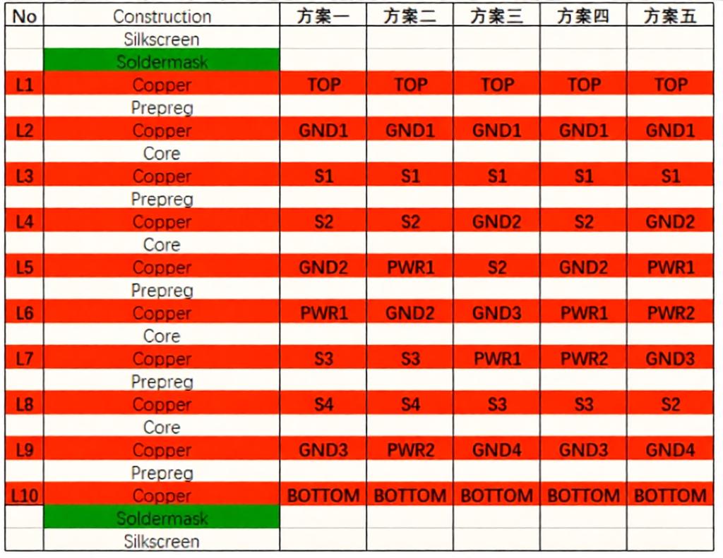
A 10-layer PCB is suitable for complex, high-density electronic systems requiring multiple power rails and excellent EMC performance.
Five common stackup configurations are available, with the primary selection criterion being the number of power planes.
For single power-plane designs, Configuration 1 is recommended. To reduce crosstalk, the spacing between Layers S1-S2 and S3-S4 should be increased.
For dual power-plane designs, Configuration 2 is preferred, and the same spacing optimization strategy should be applied.
For high-end systems requiring superior EMC performance and dual power planes, Configuration 5 offers the best overall EMC performance. Compared with Configuration 4, it sacrifices one routing layer in exchange for significantly improved electromagnetic compatibility. Layers S1 and S2 are the preferred routing layers.
Recommendation: Configuration 1 or 2 is suitable for general applications, while Configuration 5 is recommended for products with stringent EMC requirements.
12-Layer PCB Stackup
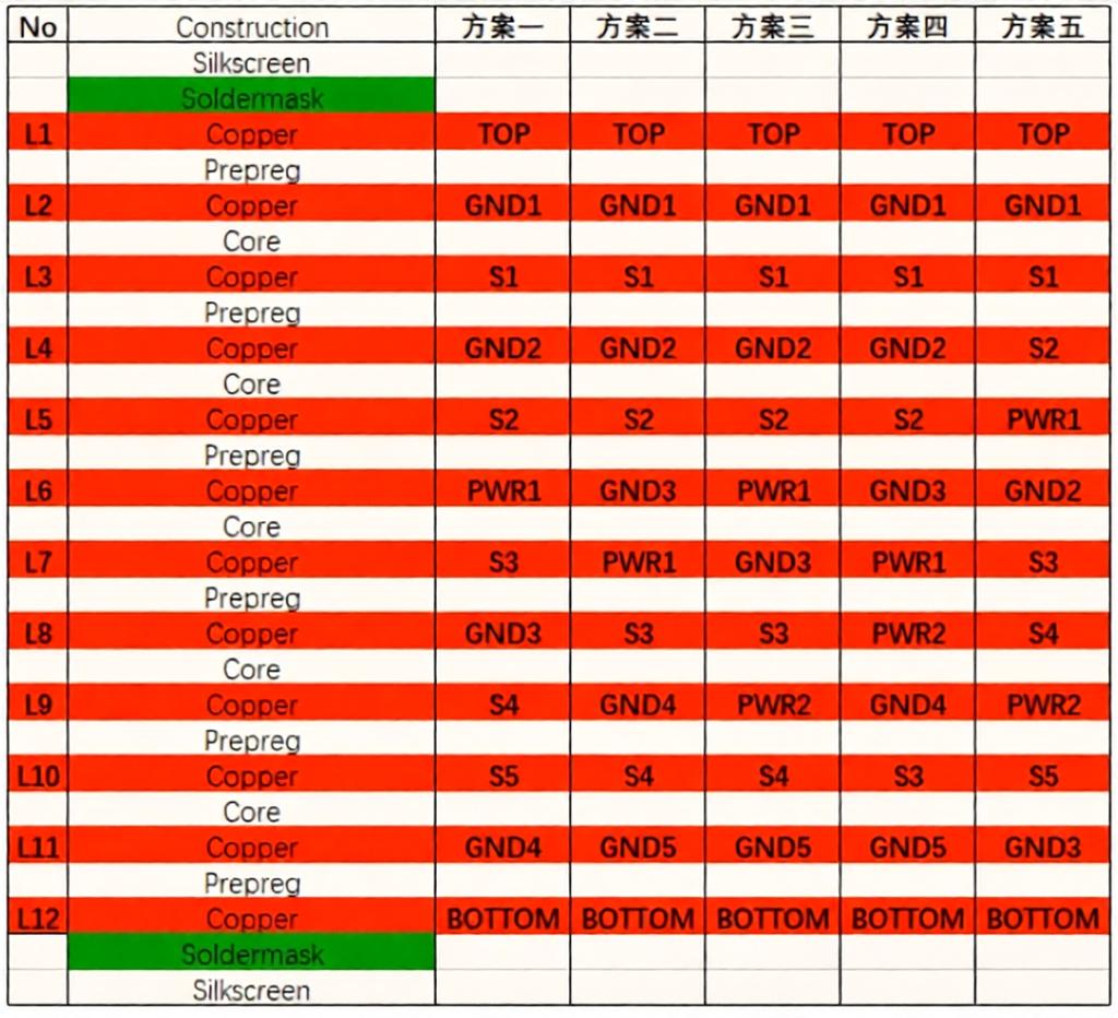
Twelve-layer PCBs are primarily used in high-speed, high-precision electronic systems with demanding EMC requirements.
Five mature stackup configurations are commonly available, each emphasizing different performance characteristics.
Configurations 2 and 4 provide outstanding EMC performance and are suitable for products that must satisfy stringent electromagnetic compatibility standards.
Configurations 1 and 3 offer an excellent balance between performance and manufacturing cost, making them ideal for most medium- to high-end applications.
Configuration 5 serves as an alternative for specialized or customized system designs.
Recommendation: Configurations 2 and 3 are generally preferred. Configurations 1 and 4 are also suitable for conventional applications, while Configuration 5 is reserved for specialized requirements.
The key to successful PCB stackup design is to build upon proven industry practices rather than developing a stackup from scratch. From basic 4-layer boards to sophisticated 12-layer designs, each stackup configuration offers distinct advantages and application scenarios. By following the fundamental principles of signal shielding, tight power-to-ground coupling, crosstalk suppression, and structural symmetry, designers can select the most appropriate stackup for their application. Combined with careful routing strategies and accurate impedance control, an optimized stackup effectively minimizes signal integrity issues, power noise, and electromagnetic interference, ensuring stable operation, regulatory compliance, and long-term reliability of the final electronic product.