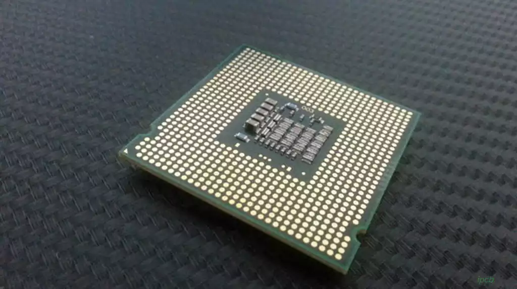
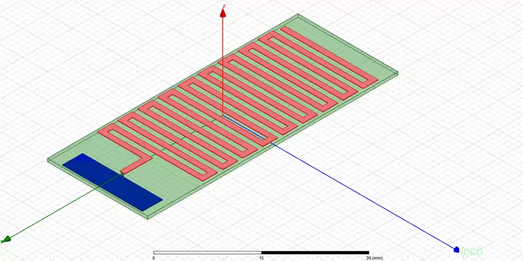
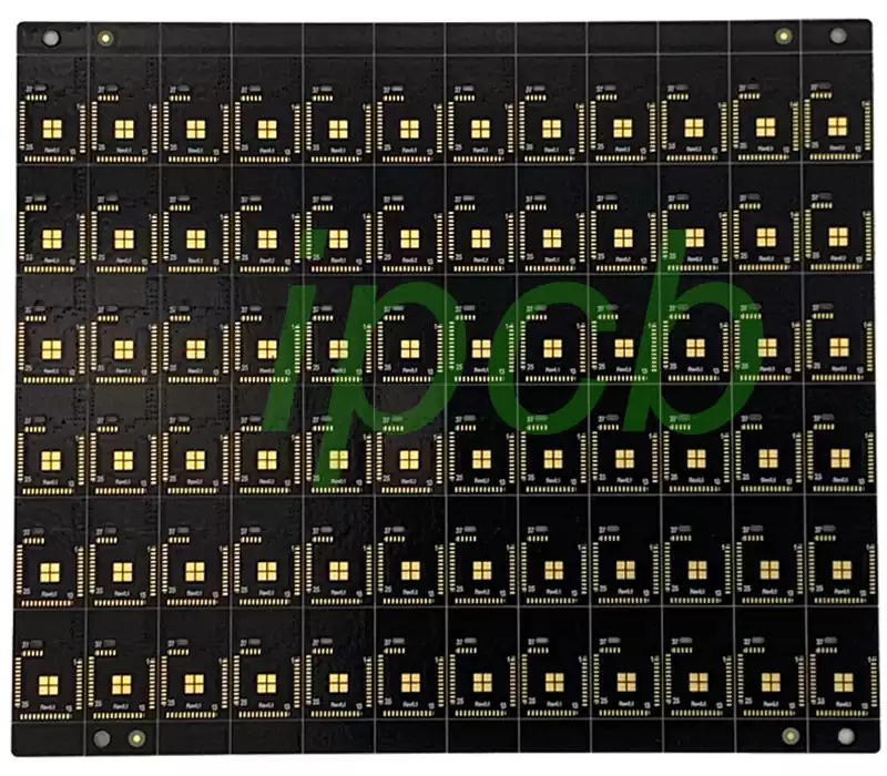
In the physical and electrical architecture of complex electronic systems (such as smartphones, laptops, industrial controllers, automotive ECUs, and servers), the PCB Main Board occupies a central and pivotal position. It is not only the physical platform for various computing units (CPU/GPU/SoC), memory chips (DDR/eMMC/NVMe), power management units (PMIC), and various RF/interface modules, but also a crucial carrier for achieving high-density signal interconnection, millivolt-level power delivery, stringent thermal management, and electromagnetic compatibility (EMC).
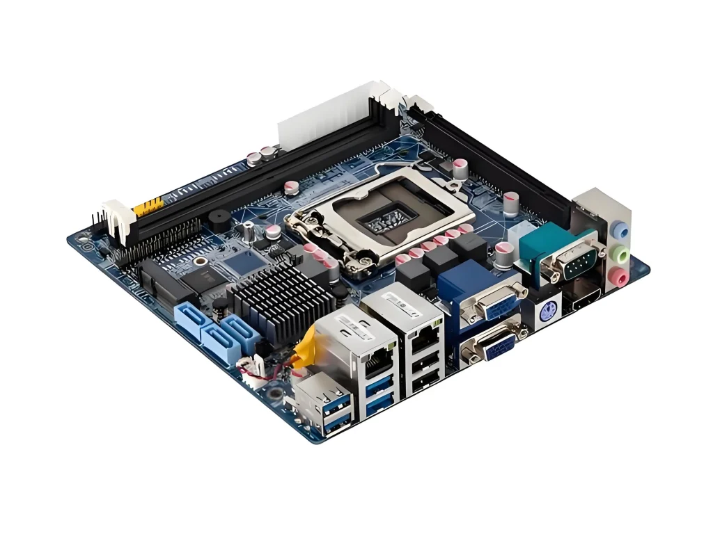
As chip manufacturing processes advance to the nanometer scale and system signal transmission rates reach tens of Gbps (such as PCIe 5.0/6.0, DDR5/DDR6, and USB4), PCB Main Board design has long since transcended the traditional scope of “wire connections,” evolving into a system-level engineering process encompassing materials physics, microwave electromagnetics, thermodynamics, electromagnetic interference control, and high-density manufacturing processes (HDI/SLP).
A deep dive into the core architecture layering, signal and power integrity design logic, high-density interconnect process evolution, and typical failure modes of the PCB Main Board is of decisive engineering value for designing highly stable and reliable electronic systems.
PCB Main Board System-Level Architecture Layering and Stack-up Design
The physical stacking design of the PCB Main Board is the cornerstone of the entire motherboard hardware engineering. An excellent multi-layer motherboard stacking structure can solve a series of problems from the physical level, such as signal cross-segmentation, excessive power impedance, and electromagnetic interference (EMI) exceeding limits.
Classic Multi-Layer Motherboard Stacking Logic and Reference Plane Principles
In modern PCB Main Boards, to ensure the continuity of characteristic impedance of high-frequency signals and provide a low-impedance current return path, the stacking design must strictly adhere to the principle of “signal layers and reference planes (GND/PWR) being adjacent.”
Core Engineering Principles of Stacking Design
In practical design, the stacking of the PCB Main Board needs to meet the following constraints:
Strong Symmetry: With the motherboard geometric centerline as the reference, the dielectric thickness, copper foil thickness, and material type of the upper and lower halves must be strictly symmetrical. If symmetry is disrupted, the motherboard will experience severe warpage and twisting due to uneven thermal expansion of the layers during the high-temperature reflow process, leading to poor soldering or cracking of BGA pads.
Tight coupling between power and ground planes: The dielectric layer between the main power plane and the main ground plane (GND plane) should be as thin as possible (e.g., 2 to 3 mil). Minimizing the physical distance between the two metal layers creates a large “plane capacitance,” providing extremely low impedance energy decoupling for the power system at high frequencies in the gigahertz (GHz) range.
Stripline shielding: Extremely sensitive weak signals or high-radiation high-speed clock lines are placed on inner signal layers (e.g., L3), sandwiched between two complete ground planes. This stripline structure completely confines the electromagnetic field between the upper and lower ground planes, providing natural electromagnetic shielding of up to 40 dB or more.
Evolution of High-Density Interconnect (HDI) and Substrate-Like Board (SLP) Manufacturing Processes
As consumer electronics and embedded devices have reached their limits in terms of size, the wiring density of main boards has undergone a qualitative leap. Traditional through-hole manufacturing technology has been completely replaced by high-density interconnect technology.
Blind and Buried Vias Technology and Stepped HDI (1+N+1 to Any-Layer)
Traditional motherboards use drills that run from the top layer to the bottom layer. This not only occupies wiring space on all intermediate layers, but through-holes also create severe “stubs” in sections where signals are not transmitted, causing strong reflections and resonances of high-frequency signals above several gigahertz.
First-order/Second-order HDI (1+N+1 / 2+N+2): Microvias (typically less than 100 micrometers in diameter) are fabricated using laser drilling technology, connecting only the top layer to the second layer or the bottom layer to the penultimate layer; the core board uses traditional buried vias.
Any-Layer HDI: Laser-drilled blind vias are used to connect any two adjacent layers on the motherboard, filled with electroplated copper (Via-in-Pad/VIPPO blind vias are drilled on the pads and filled). This structure completely eliminates through-hole mechanical vias, significantly improving the fan-out capability of pins under BGA chips and greatly reducing the physical area of the Main Board.
Subtractive Process to Semi-Subtractive Process (mSAP) and Substrate-like Board (SLP): In traditional PCB manufacturing, circuitry is formed by etching complete copper foil (subtractive process). When line width and spacing requirements are reduced to below 30 micrometers, subtractive PCBs suffer from severe under-cutting, leading to trapezoidal or even broken circuit cross-sections.
To overcome this bottleneck, modern high-end motherboards (such as top-tier smartphone motherboards) have fully adopted substrate-like PCB (SLP) technology, employing a semi-subtractive process (mSAP) for manufacturing: First, photoresist is coated onto an extremely thin copper substrate, then exposed and developed to create circuit trenches. Next, copper is “grown” into the trenches through electroplating. Finally, the photoresist is stripped and the underlying copper is removed via micro-etching. The mSAP process produces near-perfect rectangular circuit cross-sections with extremely high line width control precision, enabling PCB mainboard wiring density to approach the physical level of IC substrates.
Signal Integrity (SI) and High-Frequency Microwave Transmission Engineering
On the PCB mainboard, the essence of high-speed bus (such as PCIe, USB, MIPI, DDR) transmission is the propagation of electromagnetic waves in the transmission lines and surrounding medium. Strict physical design is essential to ensure distortion-free signal waveform delivery to the receiver.
Impedance Matching and Continuity Control: The characteristic impedance of high-speed signals is determined by conductor width, copper thickness, dielectric layer thickness, and dielectric constant (Dk). Common impedance control standards on motherboards include: single-ended 50 ohms, differential 85 ohms (PCIe standard), differential 90 ohms (USB standard), and differential 100 ohms (Ethernet/HDMI standard).
Impedance discontinuities are the root cause of signal overshoot, undershoot, and ringing. In Main Board design, all physical factors causing impedance abrupt changes must be eliminated:
Cross-split Taboo: High-speed signal lines must never cross gaps in the reference plane (such as areas where the ground plane is cut). If a cross-split occurs, the signal’s reference return path will be forced to detour, drastically increasing the return loop area, leading to a sharp rise in characteristic impedance and generating extremely strong common-mode electromagnetic radiation.
Through-through via removal (Backdrilling): For motherboards requiring through-hole vias, the excess non-signal flow stub is equivalent to an open-ended transmission line, creating a deep notch for signals in specific frequency bands. Backdrilling is necessary, using a precision-controlled mechanical drill bit to remove the excess copper via wall.
Fiber Weave Effect and Anisotropic Physical Countermeasures: The substrate of the PCB main board (such as ordinary FR-4 or low-loss materials) is woven from fiberglass cloth and impregnated with epoxy resin. Because the dielectric constant of fiberglass (approximately 6.0) is much higher than that of epoxy resin (approximately 3.0), when one parallel conductor of a high-speed differential pair rides on the fiberglass bundle and the other on the resin gap, the electromagnetic wave propagation speed on the two conductors will deviate.
This phase shift caused by dielectric anisotropy is called clock skew. It converts differential signals into common-mode signals, leading to severe signal distortion and EMI radiation.
Physical engineering solutions include:
During Main Board layout, the high-speed bus can be rotated by a certain angle (e.g., 10 to 45 degrees) for zig-zag routing;
Flat weave or open-fiber glass cloth substrates can be used to eliminate microscopic dielectric constant fluctuations.
Power Integrity (PI) and Millivolt-level Power Distribution Network (PDN)
Modern PCB Main Boards have operating voltages for main control chips (such as CPUs/SoCs) reduced to 1 volt or even below 0.8 volts, while dynamic current demands reach tens to hundreds of amperes, with extremely high current change rates (di/dt). This requires the motherboard’s Power Distribution Network (PDN) to maintain extremely low impedance (target impedance typically in the milliohm range) across an ultra-wide frequency band, from DC to several gigahertz.
Decoupling Capacitor Ladder Configuration: Individual capacitors are not ideal; their physical structure exhibits equivalent series resistance (ESR) and equivalent series inductance (ESL). To maintain low impedance across the entire frequency range, the Main Board’s power network must employ a multi-stage, ladder-like decoupling strategy:
Large-capacitance capacitors (tens to hundreds of microfarads): Placed at the output of the voltage regulator module (VRM), responsible for absorbing low-frequency (Hertz to tens of kilohertz) power ripple.
Medium-capacitance capacitors (0.1 to 1 microfarad): Placed close to the perimeter of the chip, eliminating mid-frequency (tens of kilohertz to tens of megahertz) noise.
Ultra-small capacity/low inductance capacitors (below 10 nanofarads, such as 0201 or 01005 packages): Placed directly below the BGA blind vias on the front and back of the chip (B2G/Back-to-GND), the parasitic inductance of the lines approaches zero, specifically filtering out high-frequency spike noise in the hundreds of megahertz to gigahertz range.
DC Drop (IR Drop) and High Current Thermal Effects: When carrying high currents, the resistance of the copper layer on the motherboard power plane can cause a significant DC drop. If the voltage at the chip pins drops by more than 5% due to IR Drop, it can cause logic circuits to crash. In the Main Board copper plating design, it is essential to ensure that high-current paths (such as CPU power supply VDD/CORE) have sufficient copper foil cross-sectional area (by increasing the copper plating width or using 2-ounce/3-ounce thick copper layers). Simultaneously, at high-current via arrays, the rated current carrying capacity of each via must be calculated (typically, a 15 mil mechanically drilled via has a current carrying capacity of approximately 1.5 amps) to prevent vias from burning out due to overload and overheating.
Electromagnetic Compatibility (EMC) and Grounding Physics
The PCB Main Board is the source of electromagnetic radiation emission and sensitive receiver for the entire system. Whether it can pass stringent regulatory certifications (such as FCC and CE) on the first attempt depends entirely on the EMC design of the motherboard’s underlying structure.
Grounding Strategy and Ground Loop Breaking: On the Main Board, the ground plane is not only a reference for signal return but also an electromagnetic shielding barrier. Single, Complete Ground Plane: Modern high-frequency motherboards have abandoned the earlier “analog/digital ground split” approach, replacing it with a unified, continuous, complete ground plane across the entire board. Different functional modules (such as high-sensitivity RF areas, high-speed digital areas, and high-power switching power supply areas) are isolated through physical zoning to prevent digital noise from entering sensitive areas. Via Stitching: Along the edge of the motherboard or at the junction of different functional areas, a row of densely spaced ground vias is placed at a spacing less than one-tenth of the effective wavelength of the highest signal. This forms a physical “Faraday cage,” effectively preventing high-frequency electromagnetic waves from radiating outwards from the motherboard edge (edge-rate emission shielding).
Switching Power Supply (SMPS) Hot Loop Minimization: The buck converter integrated on the PCB Main Board generates extremely high voltage change rates (dv/dt) and current change rates (di/dt) during high-speed switching of the switching transistors. The “AC current hot loop” formed by the switching transistors, freewheeling diodes, and input filter capacitors is the strongest source of electromagnetic radiation on the motherboard. During motherboard layout, the input capacitors must be placed close to the switching transistors to minimize the physical area enclosed by this hot loop, thereby cutting off the outward radiation of the electromagnetic field at its physical source.
PCB Main Board Physical Assembly and Engineering Failure Analysis
PCB Main Board After PCB fabrication and surface mount technology (SMT) are completed, the surface mount technology (SMT) components must undergo rigorous industrial-grade environmental stress screening. Due to its complex structure and dense components, it is prone to various hidden physical failures during assembly and operation.
Common Physical Failure Modes and Their Causes
[Failure Phenomenon] BGA Solder Joint Microcracks / Pad Cratering
Root Physical Mechanism: Mismatch in coefficient of thermal expansion (CTE), or excessive bending stress (Strain) on the Main Board during board-level assembly screw locking/disassembly, with stress concentrated under the highly rigid BGA pads.
Engineering Prevention Measures: Apply underfill to the four corners of the BGA to disperse stress; use strain gauges in critical areas to ensure assembly stress is less than 500 microstrain.
[Failure Phenomenon] CAF (Conductive Anode Wire) Growth Leading to Interlayer Short Circuits
Root Physical Mechanism: In a high-temperature, high-humidity environment with DC bias, copper ions migrate and precipitate from the anode to the cathode along the microscopic gaps where the glass fiber and epoxy resin are not tightly bonded, forming micron-sized metallic copper wires.
Engineering Prevention Measures: Select high-quality, CAF-resistant board material; increase the physical spacing between vias (greater than 0.3 mm) during interlayer design.
[Failure Phenomenon] Electromigration leading to surface leakage.
Root Physical Mechanism: Residual flux ions (such as chloride ions) from SMT soldering absorb ambient moisture, forming an electrolytic cell effect between adjacent conductors on the surface.
Engineering Prevention Measures: Use no-clean flux or add a high-standard conformal coating process.
Manufacturing and Assembly Checklist Filing Guidelines
Hardware and PCB engineers must complete the following final engineering checks before delivering the Main Board to production:
DFM (Design for Manufacturability) Review: Verify that the minimum trace width and spacing, minimum drill hole diameter, and Annular Ring width fully comply with the foundry’s process capability limits; check that vias fall on component pads (unless blind via copper fill process has been specified).
Design for Assemblability (DFA) Review: Ensure sufficient clearance between components of varying heights for pick-and-place nozzles; maintain adequate stress buffers around heavy-duty SMD components (such as large heatsinks and inductors).
Design for Testability (DFT) Review: Place a sufficient number of test points on all critical power rails, high-frequency clock lines, and control buses, and provide ample ground reference points on the back side for batch fault diagnosis during automated in-circuit testing (ICT).
By implementing rigorous technical controls throughout the entire process—from architecture stacking and high-density process selection to signal and power integrity calculations and EMC physical design—the PCB Main Board can demonstrate exceptional electrical performance and enduring physical reliability in the face of increasingly complex microelectronic integration challenges.