A printed circuit board capacitor may have the correct capacitance and voltage rating but still provide poor noise filtering when its PCB connection is not properly designed. At high frequencies the distance between the capacitor and the load is only part of the problem. Trace geometry via position and the ground return path determine whether the capacitor can deliver transient current quickly enough to control a local voltage disturbance.
This is why adding a printed circuit board capacitor to the schematic does not guarantee effective decoupling on the assembled board. The capacitor must form part of a short low impedance current loop. If this loop is long narrow or interrupted the parasitic behaviour of the PCB connection can dominate the electrical performance of the component.
This article explains how PCB capacitor placement affects PCB noise filtering and how to build effective local current paths around integrated circuits and switching regulators.
Why PCB Capacitor Placement Changes Filtering Performance
A decoupling capacitor acts as a local source of transient current. When an integrated circuit changes state its current demand may rise much faster than the main power source can respond through the complete PCB power distribution path.
A nearby capacitor supplies part of this short current pulse and helps prevent the voltage at the device power pin from moving outside its acceptable range.
For this process to work current must travel from the capacitor to the load and then return through the ground connection. Every pad trace and via along this path introduces parasitic resistance and inductance.
These parasitic effects become increasingly important as current changes more rapidly. A long or narrow connection can resist sudden current changes even when its DC resistance appears very low. The capacitor may therefore have sufficient nominal capacitance while being unable to respond effectively at the frequency where the noise occurs.
The practical objective of printed circuit board capacitor placement is not simply to position the component close to the IC body. The complete electrical path between the capacitor terminals and the relevant power and ground pins must be kept as compact as practical.
A capacitor that appears close in a component placement view can still be electrically distant if its connection passes through long traces distant vias or interrupted reference planes.
The Current Loop Around a Printed Circuit Board Capacitor
The capacitor current loop is the most important concept in printed circuit board capacitor placement.
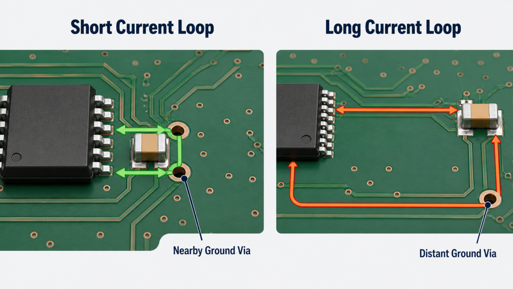
A local decoupling loop includes the capacitor power terminal the IC power pin the internal switching path the IC ground pin and the return connection to the capacitor ground terminal. The area enclosed by this capacitor current loop should be as small as practical.
A capacitor located only a few millimetres from an IC may still form a poor loop if its power trace follows a long route or its ground connection uses a distant via. Conversely a capacitor on the opposite side of the PCB may perform effectively when it is positioned directly beneath the relevant pins and connected through short nearby vias.
The connection should be direct. Power should not travel along a long trace to the IC and then branch back towards the capacitor. This arrangement places the branch and part of the supply trace inside the transient current path.
A more effective layout connects the capacitor directly across the local power and ground structure. The high frequency current can then circulate within a compact region instead of travelling through a larger area of the board.
For effective PCB noise filtering both sides of the loop must be controlled. A short power connection cannot compensate for a long or interrupted capacitor ground return path.
Trace width also matters. A narrow connection adds impedance and may allow a voltage difference to develop between the capacitor and the device pin. Short wide copper is generally preferred where component density and routing space allow it.
However the shortest geometric route is not automatically the best electrical route. The designer must also check which copper plane the connection enters whether the return path remains continuous and whether the vias are positioned in the intended current path.
Decoupling Capacitor Placement Near Integrated Circuits
Decoupling capacitor placement should begin with the power pins that experience the fastest current changes. This is particularly important for processors memories communication devices programmable logic and other ICs with rapid internal switching.
When an IC contains several power pins one capacitor may not provide an equally short current path to every pin. Local capacitors should be distributed according to the position of the power connections and the device manufacturer’s layout recommendations.
The orientation of each capacitor should support direct routing. Rotating a small surface mount capacitor can bring one pad closer to the power pin and the other closer to the ground connection. PCB capacitor placement should therefore be evaluated using pad positions rather than only the distance between component centres.
Good decoupling capacitor placement keeps both the power connection and ground return short. Optimising only one side of the loop leaves the other side free to introduce unwanted inductance.
Routing should also avoid narrow copper necks between the capacitor and the IC. A wide power region that becomes narrow at the capacitor pad still restricts the transient current path. The copper connection must remain suitable throughout the complete loop.
Every printed circuit board capacitor used for local decoupling must connect to the correct power domain. Modern ICs may contain separate rails for digital logic analogue circuits memory cores and input output functions. A capacitor connected to nearby copper from the wrong rail remains an electrical error even if its physical position appears ideal.
Component selection still matters. PCB capacitor placement cannot compensate for unsuitable capacitance voltage rating or dielectric behaviour. In the same way a correctly selected component cannot overcome a poor connection between the capacitor and the load.
Using Vias Without Adding Excessive Inductance
Multilayer PCBs commonly connect decoupling capacitors to internal power and ground planes through vias. Via location has a direct influence on the high frequency current path.
A via placed beside the capacitor pad keeps the surface connection short. If the via is positioned farther away the additional trace becomes part of the capacitor current loop and increases its impedance.
Both the power and ground vias must be considered. Placing the power via close to the capacitor while leaving the ground via on the other side of the IC can still create a large return loop.
A distant ground via lengthens the capacitor ground return path even when the power connection has been positioned correctly. Moving this via closer to the capacitor ground pad can sometimes improve the loop more than moving the capacitor itself.
For small surface mount capacitors vias can often be placed immediately beside the pads. Via in pad can provide an even more compact connection in suitable high density designs but it requires an appropriate filled and capped structure. An open via inside a solder pad can draw solder away from the joint and create an assembly defect.
Multiple vias may reduce connection impedance where current level frequency and available space justify them. Adding vias without controlling their location is less useful. Two distant vias may create a larger current path than one correctly positioned via.
The layer structure must also be considered. Closely spaced power and ground planes usually provide a more compact distribution path than reference planes separated by a thick dielectric.
A capacitor should connect to the intended reference planes without crossing splits or forcing return current around copper voids. A component can be physically close to an IC but electrically distant if the plane geometry interrupts its local return path.
Effective PCB capacitor placement must therefore be reviewed together with via position layer structure and reference plane continuity.
Capacitor Placement Around Switching Regulators
Switching regulators contain current paths with rapid changes in current. PCB capacitor placement around these circuits strongly influences supply ripple electromagnetic interference and regulator stability.
The input capacitor should be positioned close to the regulator input and power ground connections. It supplies the pulsed current drawn by the switching stage. If this high current loop is large its magnetic field and voltage disturbance can spread noise across the PCB.
The connection between the input capacitor switching device and power ground should be short and wide. Sensitive feedback and analogue traces should remain outside this noisy region.
PCB capacitor placement around a switching regulator must follow the actual pulsed current path rather than the visual outline of the regulator package. A capacitor placed close to one side of the package may still be ineffective if the relevant input and ground pins are located elsewhere.
The output capacitor should follow the current path recommended by the regulator manufacturer. Its connection to the inductor load and ground return forms part of the converter layout.
The feedback network must sense the intended output voltage rather than a noisy point carrying high current. Incorrect capacitor and feedback placement can allow switching ripple or voltage drop in the copper to influence regulation.
A capacitor should not be positioned near a switching regulator merely because unused board space is available there. Its exact location must correspond to the current loop it is intended to control.
Thermal conditions also matter. Capacitors placed beside hot inductors power semiconductors or heat sinks may operate at an elevated temperature. This is especially important for aluminium electrolytic and polymer capacitors whose characteristics and service life are temperature dependent.
PCB Capacitor Placement Errors That Increase Noise
One common mistake is arranging all decoupling capacitors in a neat row away from the IC. This may simplify the appearance of the layout but increases the individual connection length to each power pin.
A visually organised component arrangement is not necessarily good decoupling capacitor placement. Electrical current follows the copper and reference planes rather than the visual grouping of components.
Another error is focusing only on the capacitor power trace. A nearby capacitor with a distant ground via can still create a large capacitor current loop.
Connecting the capacitor through a narrow copper neck creates another restriction. The surrounding plane may appear wide but the narrow section remains part of the transient current path.
Some layouts allow the supply trace to reach the IC before branching to the capacitor. In this arrangement the printed circuit board capacitor is attached to a side branch rather than directly supporting the local power connection.
Crossing a split in the power or ground plane creates a less visible problem. Return current must travel around the split which increases the loop area and may couple noise into neighbouring circuitry.
Long routing stubs should also be avoided. A capacitor connected through a long branch can interact with trace parasitics and provide less effective suppression than expected.
These errors cannot always be identified by measuring the straight line distance between the capacitor and the IC. The complete capacitor current loop must be followed through pads traces vias power planes and the capacitor ground return path.
Reviewing PCB Capacitor Placement Before Production
Printed circuit board capacitor placement should be reviewed before production because correcting it after assembly may require routing changes rather than a simple component substitution.
The review should begin by identifying the function of each capacitor. A local decoupling capacitor a switching regulator input capacitor and a bulk storage capacitor support different current paths and should not be evaluated using one universal placement rule.
For every high frequency decoupling capacitor follow the path from the capacitor power pad to the device power pin. Then follow the return path from the device ground connection to the capacitor ground pad.
Any unnecessary trace length narrow copper distant via plane split or reference discontinuity should be examined. The review should confirm that the capacitor connects to the correct power domain and that its local return current does not cross a sensitive circuit region.
Switching regulator layouts should be compared with the component manufacturer’s recommended pattern. Small changes in the position of the input capacitor power ground and switching node can materially change PCB noise filtering performance.
Manufacturing requirements must remain part of the review. Extremely tight spacing may limit solder paste inspection automatic optical inspection and rework access. Via in pad designs require the correct filling and planarisation process. Large capacitors may require more clearance or mechanical support.
The best layout balances electrical performance with stable PCB assembly. A theoretically compact loop is not useful if it causes soldering defects or cannot be manufactured consistently.
This is where early cooperation with the PCB manufacturer becomes valuable. During engineering review iPCB can examine capacitor land patterns via structures copper connections and component clearances together rather than treating them as separate production details.
For prototype and volume PCBA projects this review can identify layouts that are electrically compact but difficult to print solder inspect or rework. Resolving these conflicts before production helps prevent a small layout weakness from becoming a repeated assembly or noise problem.
Effective Capacitor Placement Is a Board Level Decision
Reliable PCB noise filtering depends on the complete capacitor connection rather than the nominal component value alone. The finished electrical path includes the capacitor package pad geometry copper connections vias reference planes and the local ground return.
For effective decoupling the capacitor must connect to the correct power domain through a short compact loop. Both the power path and capacitor ground return path must be controlled. Placement around switching regulators requires even closer attention because rapidly changing current can spread noise through poorly arranged copper.
When customers submit PCB and PCBA data to iPCB these relationships can be reviewed together with the stack up via process solder paste requirements and inspection access. The purpose is not to redesign the customer’s circuit but to identify manufacturing details that may weaken the intended capacitor connection or reduce assembly consistency.
A printed circuit board capacitor can provide effective noise control only when its placement and interconnection support the transient current it must deliver. Treating PCB capacitor placement as part of the complete board level current path produces more reliable filtering than selecting the capacitor value alone.