In modern wireless communication, phased array radar, satellite communication, and automotive-grade millimeter-wave radar systems, RF & Microwave PCBs play a crucial and unique role. When signal operating frequencies reach hundreds of megahertz and even tens of gigahertz (GHz) in microwave and millimeter-wave bands, the traditional concepts of “wires” and “substrates” in circuit design undergo a fundamental physical evolution. Each trace on the circuit board is no longer a simple equipotential current path, but rather an electromagnetic waveguide transmission line existing with distributed parameters;
The PCB dielectric substrate is no longer merely an insulator providing mechanical support, but directly participates in signal transmission as a physical field medium for electromagnetic energy storage, coupling, and propagation. Understanding and mastering high-frequency electromagnetic theory, the physical properties of high-frequency dielectric materials, microwave transmission line impedance matching, high-frequency conductor loss mechanisms, and high-density high-frequency PCB manufacturing processes are the physical foundation for achieving high-performance, low-loss, and extremely low phase noise RF systems.
The material physics and dielectric loss mechanisms of high-frequency substrates
The primary core of high-frequency circuit board design lies in the physical selection of the substrate. FR-4 substrates, widely used in low-frequency circuits, are made of cross-woven epoxy resin and glass fiber. While their physical topology is macroscopically uniform, they appear extremely non-uniform to microscopic electromagnetic waves. More importantly, FR-4 material exhibits a large dielectric loss tangent and severe dielectric constant dispersion in the gigahertz band. When high-frequency electromagnetic waves pass through the FR-4 substrate, the high-frequency dipoles of the resin molecules violently oscillate and rub against each other, converting a large amount of electromagnetic wave energy into heat, leading to a sharp signal attenuation. Therefore, microwave and millimeter-wave circuits must rely on dedicated high-frequency inorganic or polymer substrates.
The core physical property of high-frequency substrates is primarily the stability of their relative dielectric constant with frequency and temperature. The dielectric constant directly determines the propagation phase velocity of electromagnetic waves in the medium and the characteristic impedance of the transmission line. When broadband radio frequency signals (such as 5G millimeter-wave or ultra-wideband radar signals) propagate on a circuit board, if the dielectric constant of the substrate shifts at different frequency components (i.e., dispersion), electromagnetic waves of different frequencies will propagate at different speeds, resulting in severe phase shift distortion and envelope dispersion in the time domain at the receiving end. Furthermore, the rate of change of the substrate’s dielectric constant with ambient temperature (TcC) is equally critical. For microwave systems deployed in extreme environments such as outdoor base stations or aerospace, temperature-induced dielectric constant drift directly disrupts the tuning frequencies of microwave filters and phased array antennas.
The dielectric loss tangent is another key physical parameter determining the thermal attenuation of high-frequency signals. Dielectric loss is directly proportional to the operating frequency of the electromagnetic wave; the higher the frequency, the faster the polarization reversal of the dielectric molecules, resulting in more severe loss. High-end microwave substrates, such as polytetrafluoroethylene (PTFE) and hydrocarbon ceramic polymers, utilize extremely pure nonpolar molecular structures to reduce the dielectric loss tangent to extremely low levels, thus ensuring low signal attenuation in long-distance transmission or complex microwave networks. High-power RF amplifier modules also release a significant amount of heat to the circuit board, requiring high-frequency substrates to not only have extremely low dielectric loss but also excellent thermal conductivity to rapidly conduct the junction temperature of power devices away. Simultaneously, the coefficient of thermal expansion of the substrate in the direction perpendicular to the board surface (Z-axis) must be highly matched with the copper foil and the copper layer of the metallized via walls. Otherwise, under repeated thermal cycling and high-power impacts, the enormous thermal stress loss will cause microscopic fractures in the via metallized layer, resulting in overall board failure.
Microwave Transmission Line Topology and Electromagnetic Field Physical Distribution
In high-frequency circuit boards, the electromagnetic field is not confined to the metal traces but is extensively distributed in the surrounding medium and space. Choosing a suitable transmission line topology directly determines the distribution of the electromagnetic field, radiation loss, and isolation from other circuits. Common microwave transmission line topologies mainly include microstrip lines, striplines, and grounded coplanar waveguides.
A microstrip line consists of metal traces arranged on the PCB surface and a complete main ground plane located below, isolated by a high-frequency dielectric layer. The physical topology of the microstrip line determines that its electromagnetic field exhibits a quasi-TEM mode distribution, with part of the electromagnetic wave propagating in the underlying high-frequency dielectric and the other part exposed to the air. The biggest engineering advantage of microstrip lines lies in their extremely convenient testing and debugging, intuitive component placement, and relatively low overall conductor and dielectric losses due to the single dielectric layer. However, because a portion of their electromagnetic field extends into the upper air layer, microstrip lines are prone to radiating electromagnetic interference and are also highly susceptible to the physical effects of external metal shielding, housings, and even ambient humidity.
Striplines, on the other hand, completely embed the metallic signal traces within a uniform dielectric layer between two parallel ground planes. Striplines transmit pure TEM mode electromagnetic waves, with the two complete metal ground planes forming an absolutely closed physical shielding space. This structure gives striplines natural electromagnetic barrier properties, preventing electromagnetic energy radiation into the external space and absorption of interference from other sensitive modules on the same board. Therefore, they are extremely suitable for wiring multiple densely parallel lines, such as in phased array radar. However, the disadvantage of striplines is that signals must be transmitted from the surface to the inner layer via microwave vias. The vias themselves introduce parasitic capacitance and inductance, disrupting the continuity of the transmission line’s characteristic impedance. Furthermore, striplines are encapsulated within upper and lower dielectric layers, making manual soldering, debugging, and modification virtually impossible later.
Grounded Coplanar Waveguides (GCPWs) are based on microstrip lines, with large-area ground copper foils laid flat on both sides of the signal trace on the same layer. Precisely controlled physical gaps are maintained between the signal line and the ground copper foils on both sides, while retaining a complete main ground plane underneath. Electromagnetically, grounded coplanar waveguides tightly confine most electromagnetic lines of force within the narrow gap in the dielectric between the signal line and the ground copper foils on both sides of the same layer. For millimeter-wave frequencies above tens of gigahertz, the confinement force of grounded coplanar waveguides is far stronger than that of ordinary microstrip lines, significantly reducing energy loss due to spatial radiation and greatly suppressing parasitic electromagnetic crosstalk between adjacent high-frequency traces. By adjusting the ratio of the side gaps to the trace width, engineers can flexibly control the characteristic impedance of the transmission line without drastically changing the dielectric layer thickness of the PCB.
High-Frequency Skin Effect, Surface Roughness, and Conductor Plating Physics
Besides dielectric substrate loss, another major contributor to attenuation in high-frequency circuit boards comes from the physical losses of the metal conductor itself. Under DC or low-frequency AC conditions, electrons flow relatively uniformly across the entire cross-section of a copper conductor. However, as the signal frequency increases, the changing magnetic field inside the conductor induces eddy currents. The magnetic field generated by these eddy currents, in turn, cancels out the current in the central region of the conductor, forcing the current to gradually concentrate on the microscopic surface of the conductor. This physical phenomenon is known as the skin effect.
As signal frequencies enter the millimeter-wave band, the skin depth of the current shrinks dramatically to the submicron level. This means that the higher the frequency, the thinner the actual physical thickness of the copper layer involved in conduction, and the effective equivalent resistance of the conductor increases exponentially. Due to the skin effect, high-frequency current actually only flows through the microscopic surface at the interface between the copper foil and the dielectric layer. At this point, the microscopic roughness of the copper foil surface has a decisive physical influence on conductor losses.
In PCB manufacturing, to enhance the physical-mechanical adhesion between the copper foil and the high-frequency resin dielectric, traditional copper foil surfaces are typically chemically treated to create a microscopically uneven copper tooth structure. For low-frequency signals, this microscopic roughness is negligible; however, for ultra-high-frequency radio frequency signals with a skin depth of only a few tenths of a micrometer, the high-frequency current is forced to flow along these uneven microscopic copper tooth zigzags. The actual physical path of the current is significantly lengthened, resulting in a dramatic increase in physical resistance and consequently an exponential increase in conductor loss on the transmission line. Therefore, in high-frequency PCBs used in the millimeter-wave band, ultra-low roughness (VLP) or even high-volume low roughness (HVLP) copper foil must be specified to control the microscopic roughness of the copper foil surface to an extremely small sub-micrometer level, ensuring a flat and low-attenuation high-frequency electromagnetic wave transmission path.
Furthermore, the metal plating process on the circuit board surface also has a direct physical destructive or protective effect on high-frequency performance. The commonly used chemical engraving (ENIG) surface treatment for low-frequency circuit boards involves a layer of metallic nickel between a nickel layer and a gold layer. However, nickel is a typical ferromagnetic metal with a much higher relative permeability than copper. High-frequency electromagnetic waves in the nickel layer generate extremely strong hysteresis losses and huge skin resistance, known as “nickel losses.” In the RF trunk area above 6 GHz, if the impedance lines are covered by an ENIG plating, the insertion loss of high-frequency signals will deteriorate drastically. Therefore, the surface treatment of high-frequency circuit boards usually strictly avoids ENIG, instead using highly conductive and non-magnetic processes such as immersion silver or immersion tin, or electroplating pure gold in the pad areas to maintain perfect physical conductivity of high-frequency transmission lines.
Hybrid laminated structures and high-precision manufacturing engineering
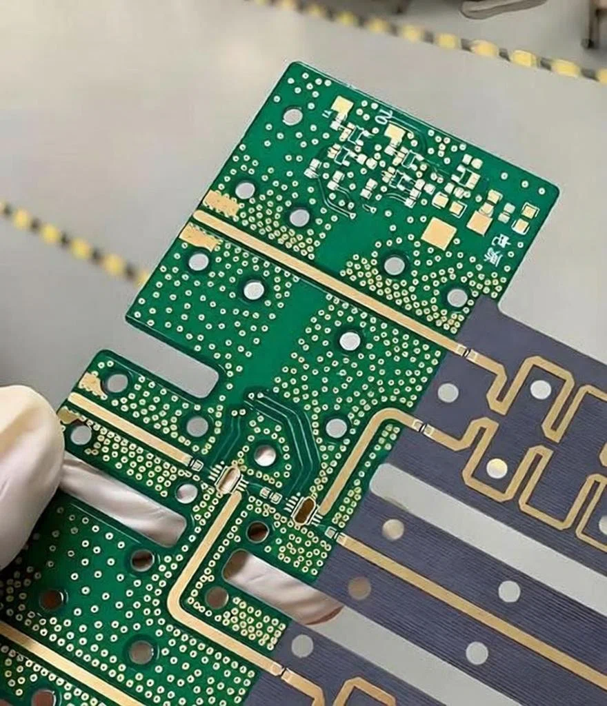
High-frequency microwave substrates (such as Rogers or Taconic series) are extremely expensive, and multilayer boards made of pure high-frequency materials present significant processing challenges in terms of mechanical rigidity, multilayer lamination strength, and thermal expansion coefficient control. To achieve the optimal balance between electrical performance and production costs, the industry widely employs hybrid stack-up technology, combining high-frequency materials with standard FR-4 substrates.
In a typical hybrid stack-up structure, the entire board is not made of high-frequency substrate. Engineers use a thin high-frequency core only for critical layers containing high-frequency RF microstrip or stripline lines (e.g., between the top and second layers), while the underlying structure, used for power lines, low-frequency control lines, and digital signal lines, continues to use inexpensive, high-strength standard FR-4 substrate and prepreg. This physical structure ensures that RF signals propagate only in the extremely low-loss high-frequency medium and significantly reduces the overall material procurement cost and manufacturing complexity.
However, hybrid stack-up presents significant challenges to PCB foundries’ manufacturing processes. Because the molecular structure, coefficient of thermal expansion, and flow characteristics of the high-frequency core board material and the FR-4 material are drastically different, the rates of thermal expansion and contraction of the two materials are inconsistent during the high-temperature, high-pressure multilayer board lamination process. This can easily lead to severe board bending, warping, and even interlayer delamination in the finished circuit board. The foundry must precisely calculate and adjust the physical parameters of the lamination temperature rise curve and pressure gradient, and use flow-deep-free prepregs to ensure high-precision control of the dielectric layer thickness.
Besides the lamination process, high-frequency microwave transmission lines are extremely sensitive to geometric tolerances. For a high-frequency microstrip line designed with a characteristic impedance of 50 ohms, a tiny tolerance deviation of only ten micrometers in the physical width of the trace during etching can directly cause an impedance shift of several ohms. This impedance discontinuity will cause electromagnetic wave reflections on the high-frequency signal transmission path, resulting in a significant deterioration in reflection loss (S11) and the formation of standing waves on the transmission line, thus compromising the power transmission efficiency of the entire RF front-end. To control this deviation, high-frequency PCB manufacturing must abandon traditional optical exposure etching and fully adopt laser direct imaging (LDI) technology and high-precision vacuum-compensated etching processes to strictly lock the width and spacing tolerances of finished traces within the micrometer-level error range.
Signal Layer-Changing Back-Drilling Process and Via Parasitic Effect Control
In multilayer high-frequency PCB design, radio frequency signals often need to physically shuttle between different wiring layers through metallized vias, such as changing from a surface microstrip line to an inner stripline. However, from a high-frequency electromagnetics perspective, a typical via structure is actually a complex network of distributed parameters, containing parasitic capacitance and inductance, which can cause significant impedance abrupt changes at the via location.
An even more serious problem arises from the parasitic stubs of vias. When a signal is transmitted from the top layer (layer 1) through a via to an inner layer (e.g., layer 3), the section of metal pillar in the via wall from layer 3 to the bottom layer (e.g., layer 12) through which no current flows constitutes a via stub. In low-frequency circuits, this parasitic metal stud is negligible; however, in the high-frequency microwave band, it is physically equivalent to an open-ended transmission line. According to microwave transmission line theory, when the physical length of the stud is exactly one-quarter of the signal wavelength, it generates strong electromagnetic resonance at a specific frequency, causing its equivalent input impedance to approach zero.
This means that a quarter-wavelength stud becomes a physical “short-circuit point” or notch filter at a specific high-frequency point, reflecting or attenuating all RF signals in that band, resulting in a large deep hole in the signal transmission frequency response curve. To eliminate the devastating impact of parasitic studs on high-frequency signals, high-precision backdrilling must be introduced into high-frequency PCB manufacturing. Backdrilling involves using a secondary drill bit, slightly larger in diameter than the original drill bit, to precisely control the drilling depth from the back of the circuit board after the vias are plated in the multilayer board, completely removing the excess copper metal walls of the vias that do not carry signals. By compressing the physical length of the residual pile through the hole to an extremely small limit, the resonance notch phenomenon can be completely eliminated, ensuring that high-frequency signals maintain good broadband signal integrity when transmitted across layers.