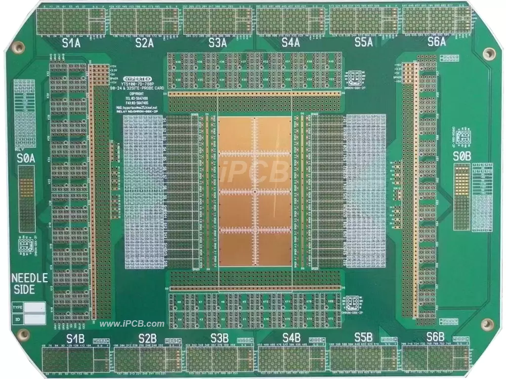
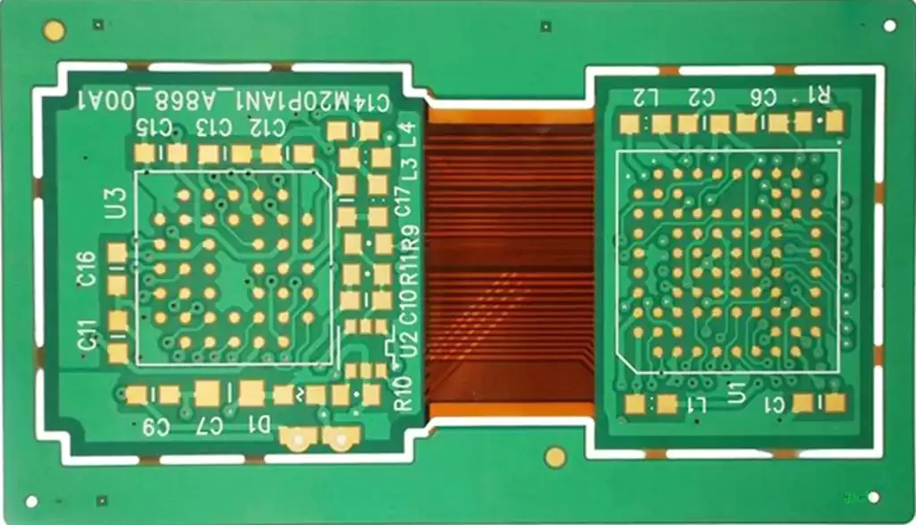
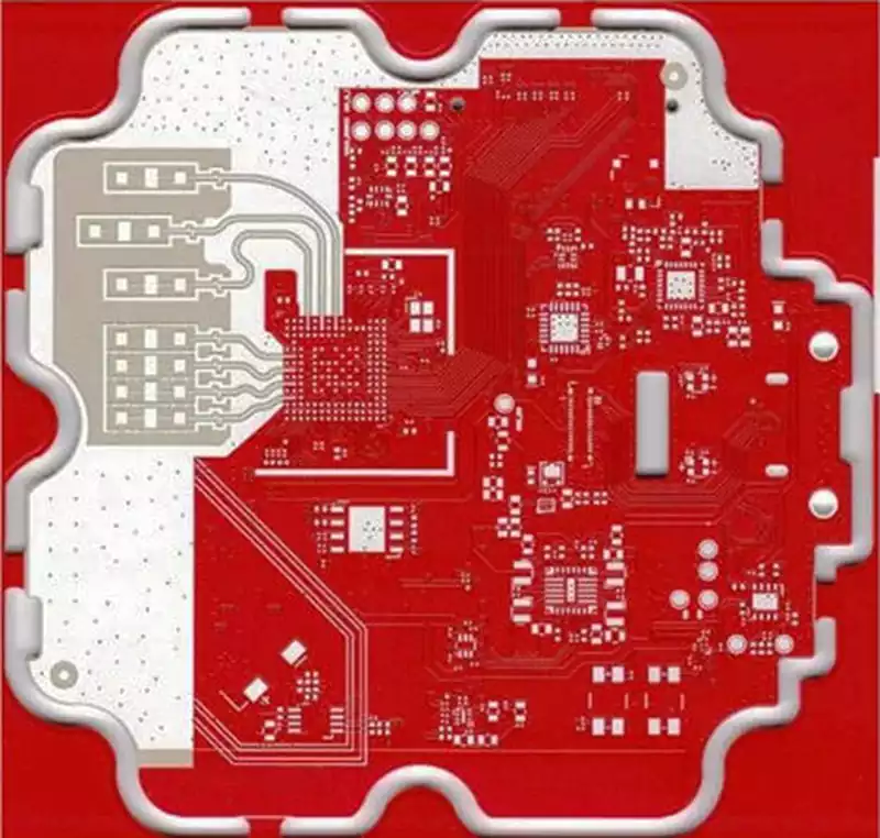
A prototype printed circuit board is one of the most important physical stages in electronic product development. It transforms a schematic and PCB layout into an actual board that engineers can assemble, power, measure, modify, and test under real operating conditions.
A PCB prototype is not simply a smaller version of a production order. Its primary purpose is to answer engineering questions before a product moves into larger-scale manufacturing. Engineers may use a prototype to verify circuit functionality, check component placement, evaluate mechanical fit, measure electrical performance, identify layout problems, and determine whether the design can be manufactured consistently.
This distinction matters because a PCB can appear correct in a design file and still behave differently when it becomes a physical product. Trace geometry, component tolerances, thermal behavior, connector placement, assembly constraints, and interactions between different parts of the board can introduce problems that are difficult to identify from the schematic alone.
Recent research on rapid PCB prototyping also emphasizes early testing, incremental iteration, and designing prototypes specifically to answer defined engineering questions rather than treating the first PCB as a nearly finished product.
What Is a Prototype Printed Circuit Board?
A prototype printed circuit board is a low-volume PCB manufactured to evaluate an electronic design before the design enters regular production. It may be produced in only a few pieces or in a small engineering batch, depending on the project and the amount of testing required.
The physical board can be manufactured using the same fundamental PCB fabrication technologies used for production boards. The difference is mainly the purpose, quantity, development stage, and manufacturing priorities.
A prototype printed circuit board is usually produced when an engineering team has reached a point where simulations and design reviews are no longer sufficient. The team needs a physical board to determine whether the electrical design works as expected and whether the PCB can be assembled and integrated into the final product.
This is why prototype printed circuit boards are particularly valuable during new product development. They provide physical evidence that can be compared with the original design assumptions.
Why prototype printed circuit boards Matter in Electronic Product Development
The earlier a design problem is discovered, the easier it is usually to correct. Changing a schematic or PCB layout before manufacturing is generally much less disruptive than discovering the same problem after a production run has already been completed.
A prototype provides an opportunity to identify these issues while changes are still relatively manageable.
For example, an engineer may discover that a connector interferes with the enclosure, that a heat-generating component needs a different thermal path, or that a particular signal becomes unstable because of the PCB layout. A prototype can also reveal assembly problems that were not obvious during design, such as insufficient component clearance or a footprint that is difficult to manufacture or inspect.
The value of a prototype therefore comes from the information it generates, not simply from producing a physical board.
A recent 2026 study of rapid PCB prototyping recommends using prototypes as instruments for learning, increasing fidelity deliberately, iterating incrementally, and testing early rather than waiting until a highly developed design is complete.
What Should Be Verified With a prototype printed circuit board?
Electrical Function
The first question is usually whether the circuit performs its intended function. Engineers can power the prototype, measure voltages and currents, observe signals, and compare actual behavior with simulation or design expectations.
This stage may expose incorrect component values, unexpected interactions between circuit blocks, power distribution problems, signal integrity issues, or firmware-related hardware behavior.
PCB Layout
A prototype also provides an opportunity to evaluate the physical implementation of the circuit. Component placement, routing, grounding, power distribution, connector locations, and test points can all be assessed using the physical board.
For high-speed, RF, or mixed-signal designs, this becomes especially important because the physical structure of the PCB can directly influence electrical performance.
Mechanical Fit
Electrical functionality is only one part of product development. The prototype should also be checked against the enclosure, mounting points, connectors, cables, switches, displays, and other mechanical components.
A board that functions perfectly on a laboratory bench may still require another design iteration if it cannot fit correctly into the intended product housing.
Thermal Performance
Prototype testing can reveal how components and PCB areas behave under actual operating loads.
Power amplifiers, processors, regulators, LEDs, motor-control components, and other heat-generating devices may produce temperature distributions that are difficult to predict accurately without physical testing.
Thermal measurements can therefore influence component placement, copper areas, thermal vias, heatsinks, airflow, and even the PCB material or stackup.
Assembly Feasibility
The prototype can also reveal whether the board is practical to assemble. Component spacing, package selection, pad geometry, soldering access, polarity markings, and inspection accessibility can all influence assembly.
This is where Design for Manufacturability becomes particularly valuable. IPC describes DFM as an important part of product development and provides design rules derived from standards including IPC-2221, IPC-2222, IPC-2226, IPC-2152, IPC-6012, and IPC-7351.
Prototype printed circuit boards vs Production PCB
The difference between a prototype PCB and a production PCB is primarily related to their role in product development rather than the basic concept of the board itself.
A prototype is produced to learn whether the design works and what needs to change. Production boards are manufactured after the design has been sufficiently validated and are optimized around repeatability, yield, cost, supply-chain requirements, and long-term manufacturing stability.
This does not mean that a prototype should be designed without regard to production requirements. In fact, the closer a prototype is to the eventual manufacturing configuration, the more useful it can be when the purpose is to validate production readiness.
However, there are situations where deliberately simplified prototypes make sense. A development team may use a less complex board to answer a specific electrical question before investing time in a complete production-level design.
The important point is to understand what each prototype is intended to prove.
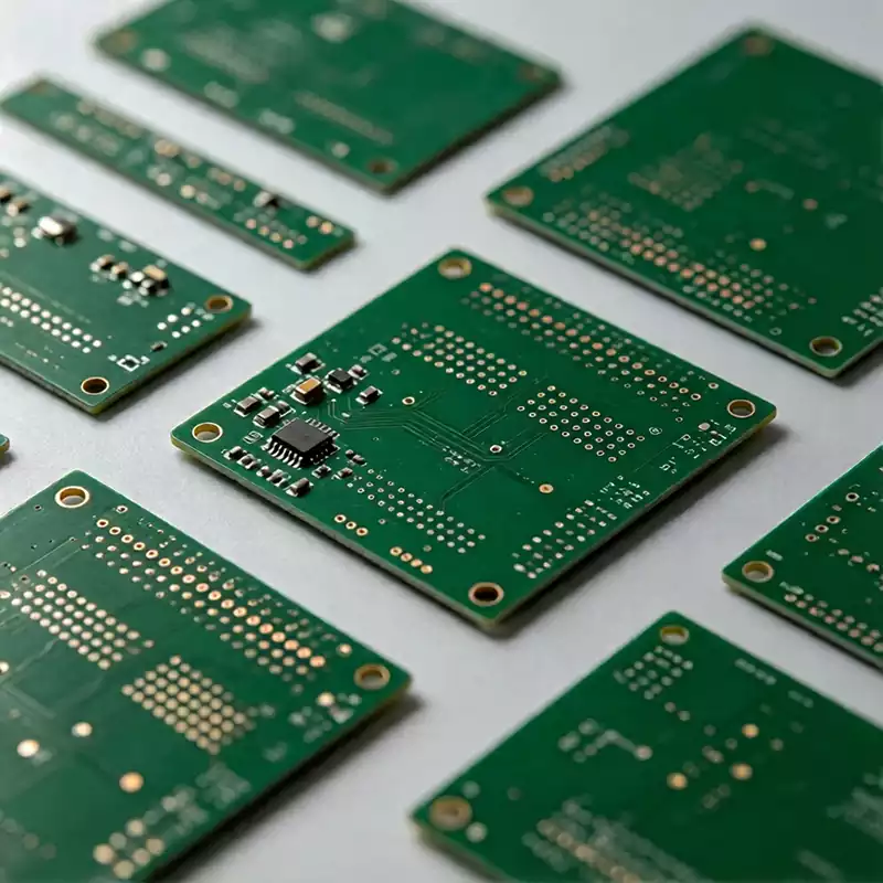
The PCB Prototype Development Process
A successful prototype normally begins before the PCB files are sent to a manufacturer. The design team first needs to define what the prototype is expected to validate.
Define the Engineering Objectives
The prototype should have a clear purpose. If the main question concerns power consumption, the design and test plan should make power measurements easy. If the main concern is RF performance, the board should provide appropriate RF test structures and controlled transmission paths.
A prototype with no defined validation objectives can become expensive without producing useful information.
The 2026 research on rapid PCB prototyping makes a similar recommendation: prototypes should be designed around specific questions, with unnecessary complexity reduced where possible.
Complete the Schematic
Once the engineering objectives are clear, the schematic defines the electrical relationships between components.
Component selection should consider not only electrical specifications but also package availability, lifecycle, tolerances, thermal characteristics, and assembly requirements.
For prototypes, component availability can be particularly important because a technically suitable component that cannot be sourced quickly may delay the entire development cycle.
Create the PCB Layout
The PCB layout translates the schematic into a physical structure. Component placement and routing should reflect the electrical requirements of the design rather than simply attempting to fit every component into the available space.
Critical power paths may require wider conductors, sensitive analog circuits may require controlled return paths, and high-speed or RF signals may require impedance-controlled structures.
The layout should also consider manufacturing constraints before the prototype is fabricated. Autodesk’s guidance on producing working PCB prototypes highlights component placement, trace widths, EMI considerations, power and ground planes, and documentation as important design decisions affecting prototype success.
Perform Design Verification
Before fabrication, the PCB design should be reviewed for obvious errors and manufacturing risks.
Depending on the design, this may include electrical rule checking, design rule checking, signal-integrity analysis, thermal analysis, impedance calculation, component clearance verification, and DFM review.
This stage is particularly useful because a prototype is not an excuse to skip engineering verification. The purpose of the prototype is to investigate remaining uncertainties, not to manufacture a board containing avoidable design errors.
Manufacture the PCB Prototype
Once the design files are ready, the PCB manufacturer fabricates the bare boards according to the specified layer count, material, copper thickness, surface finish, minimum trace and spacing requirements, via structure, and other fabrication requirements.
The manufacturer may also review the design before fabrication and identify potential manufacturing concerns.
IPC’s PCB standards distinguish between design requirements and performance requirements, and IPC-A-600 provides acceptability criteria for printed boards.
Assemble and Test the Board
The bare PCB becomes a functional prototype only after components have been assembled and the board has been tested.
Depending on the project, assembly may involve SMT placement and reflow soldering, through-hole assembly, selective soldering, manual rework, or a combination of these processes.
Testing should then be performed against the objectives established at the beginning of the prototype cycle.
How Many Prototype printed circuit boards Should Be Ordered?
There is no universal quantity that works for every project.
The number of prototype printed circuit boards should depend on the complexity of the design, the number of tests required, the probability of design changes, component availability, and whether destructive or environmental testing is involved.
A single board may be sufficient for a simple proof-of-concept experiment, but a more complex product may require multiple units for electrical validation, mechanical testing, firmware development, reliability testing, and engineering rework.
Ordering a few additional boards can also be useful when the cost of another fabrication cycle is significant compared with the incremental cost of producing extra prototypes.
The goal should not simply be to minimize prototype quantity. It should be to obtain enough physical units to answer the important engineering questions without unnecessarily increasing development cost.
PCB Materials for Prototyping
The material used for a prototype should reflect what the board is expected to do.
FR-4 remains a common choice for many general-purpose PCB prototypes because of its established manufacturing process and broad application range. However, it is not automatically the correct choice for every design.
High-frequency circuits may require materials with more tightly controlled dielectric characteristics and lower loss. High-temperature applications may require materials with different thermal properties, while flexible products require an appropriate flexible substrate.
Using a different material for the prototype than the eventual production board can sometimes reduce the value of testing because electrical or thermal behavior may change when the substrate changes.
For this reason, the prototype material should be selected according to the specific question being tested. When the objective is production validation, using the intended production material is generally more meaningful.
Prototype printed circuit boards Design for Manufacturing
One of the most common mistakes in PCB prototyping is treating manufacturability as something that can be addressed after the layout is finished.
A design may be electrically correct but unnecessarily difficult to fabricate or assemble. Very tight spacing, unusual board thicknesses, difficult component packages, insufficient copper clearance, poorly positioned vias, and inaccessible test points can all create manufacturing problems.
DFM review helps identify these issues before fabrication. IPC’s DFM guidance specifically addresses design requirements across different PCB complexity and performance levels.
For a prototype, DFM is valuable for another reason: it can make the transition to production smoother. If the prototype has already been designed around realistic manufacturing constraints, fewer changes may be required when the project moves toward larger production quantities.
Design Features That Make PCB Prototypes Easier to Debug
A prototype should be designed for measurement and modification.
Accessible test points can make it easier to measure critical voltages and signals. Clearly marked reference designators and polarity indicators can reduce assembly and debugging errors. Where appropriate, solder jumpers, configuration resistors, programming headers, and removable connectors can make it easier to change the board without producing another PCB immediately.
The 2026 research on rapid PCB prototyping specifically recommends accessible test points, solder pads, through-holes, and hand-solderable packages when these features help engineers troubleshoot and modify early prototypes.
These features may not all be necessary on a final production board, but they can significantly increase the value of an engineering prototype.
Common Problems Found During PCB Prototyping
Prototype testing frequently reveals issues that were not obvious during schematic and layout development.
One common problem is incorrect component placement. A component may be electrically connected correctly but physically interfere with another component, enclosure, connector, or heatsink.
Another issue involves signal integrity. High-speed traces may exhibit unexpected reflections, crosstalk, or timing behavior when the actual PCB structure differs from the assumptions used during design.
Power distribution can also cause problems. Voltage drops, ground noise, insufficient copper, or poor decoupling can produce unstable behavior that is difficult to reproduce in simulation.
Thermal problems may appear when the prototype operates continuously under real load. Components that seemed acceptable based on their nominal power ratings may require additional copper, improved thermal paths, or different placement.
Assembly problems are another important category. A footprint can be technically correct while still being difficult to inspect, solder, rework, or place consistently.
These issues are not necessarily evidence that prototyping has failed. They are precisely the kinds of problems that a prototype is intended to expose before production.
How to Reduce PCB Prototype Iterations
The goal of prototyping is not necessarily to eliminate every design iteration. Some iteration is expected, particularly for new or technically uncertain products.
A more useful objective is to make each iteration answer a specific engineering question.
Instead of changing the circuit, PCB layout, component selection, and mechanical structure simultaneously, engineers can isolate major variables where practical. This makes it easier to understand why a particular version succeeded or failed.
The latest research on rapid PCB prototyping recommends incremental iteration and changing major variables deliberately rather than combining too many unproven design changes into one prototype.
Simulation can also reduce unnecessary fabrication cycles. However, simulation should complement physical prototyping rather than replace it when the design depends on physical characteristics that are difficult to model accurately.
From prototype printed circuit boards to Production
The transition from prototype to production is not simply a matter of increasing the order quantity.
Once the design has been validated, the manufacturing team needs to evaluate whether the board can be produced consistently at the required volume. This can involve reviewing material availability, component sourcing, fabrication tolerances, assembly yield, test procedures, panelization, tooling, inspection, and production cost.
Some prototype designs need to be modified before production because they were intentionally optimized for engineering access rather than manufacturing efficiency.
For example, a prototype may contain additional test points, hand-solderable components, configuration jumpers, or other debugging features that are unnecessary in the final product. Other changes may be required because a component is difficult to source at production volume.
The transition should therefore be treated as a controlled engineering stage rather than an automatic continuation of prototyping.
Why DFM Matters Before Ordering a Prototype
A prototype is often ordered under time pressure, but skipping a manufacturing review can create avoidable delays.
A DFM review can identify issues involving trace width, spacing, holes, copper distribution, board thickness, component clearance, solder mask, silkscreen, and assembly accessibility before the board enters fabrication.
This is especially important for complex boards such as HDI, high-density SMT assemblies, RF boards, and high-speed designs where manufacturing tolerances can directly influence electrical performance.
IPC’s DFM framework provides design profiles based on PCB performance classes and producibility levels, reinforcing the idea that manufacturability should be considered during design rather than after the PCB has already been produced.
Prototype Printed Circuit Boards for Complex Applications
The requirements of a prototype become more demanding as the electronic system becomes more complex.
For RF designs, the prototype may need controlled impedance, specific dielectric materials, carefully defined ground structures, and appropriate RF test interfaces.
High-speed digital boards may require controlled-impedance routing, carefully designed power distribution, low-noise reference planes, and signal-integrity validation.
Power electronics may require larger copper structures, thermal vias, appropriate substrate selection, and thermal testing.
HDI designs may introduce microvias, fine-pitch components, sequential build-up structures, and tighter manufacturing tolerances.
In these cases, a prototype should reproduce the critical physical characteristics of the intended production design closely enough for the test results to be meaningful.
Prototype PCB Manufacturing With a PCB Manufacturer
The relationship between the engineering team and PCB manufacturer can have a significant impact on prototype development.
The manufacturer should understand the intended layer count, material system, copper requirements, surface finish, controlled-impedance requirements, via structures, minimum feature sizes, and assembly expectations before production begins.
Clear documentation reduces the possibility of assumptions being made during fabrication.
For complex prototypes, it can also be useful to discuss manufacturing constraints before the layout is finalized. A PCB manufacturer may identify a fabrication issue early enough for the designer to modify the layout without affecting the entire development schedule.
This approach is particularly valuable when the prototype uses advanced materials, fine-line structures, HDI technology, controlled impedance, or unusual mechanical requirements.
At iPCB, prototype printed circuit board projects can be evaluated from both fabrication and assembly perspectives, allowing engineering teams to consider PCB manufacturing constraints before moving into the prototype build. For projects that are expected to progress toward production, the prototype stage can also be used to identify DFM issues and establish a more practical path toward volume manufacturing.