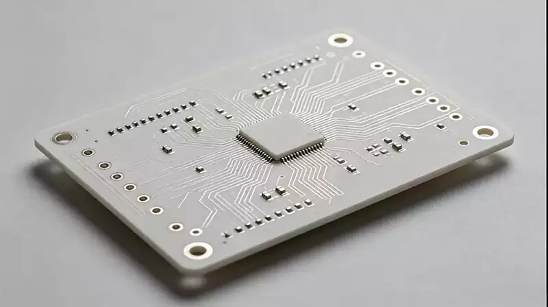
Multilayer ceramic pcbs combine the electrical integration advantages of multilayer circuitry with the excellent thermal conductivity, mechanical strength, and high-temperature resistance of ceramic substrates. Unlike single-layer ceramic PCBs, which are limited to routing circuits on the surface of the substrate, multilayer ceramic PCBs can integrate multiple circuit layers within the ceramic substrate. This enables engineers to design shorter signal paths and more compact circuit structures while achieving internal electrical interconnections that are not possible with conventional single-layer ceramic boards.
As electronic equipment continues to evolve toward smaller form factors and higher performance, many electronic components face challenges such as limited installation space, high heat generation, demanding high-frequency signal transmission, and complex operating environments. The structural advantages of multilayer ceramic PCBs become particularly valuable in these applications. Alumina and aluminum nitride are currently the two most widely used ceramic substrate materials, while High-Temperature Co-Fired Ceramic (HTCC) and Low-Temperature Co-Fired Ceramic (LTCC) are the two established manufacturing technologies for multilayer ceramic circuit structures.
It is important to understand that a multilayer ceramic PCB is not simply a conventional FR-4 multilayer PCB with a different substrate material. From the material system, conductor formation, and via fabrication to layer stacking, lamination, sintering, dimensional control, and surface metallization, every stage follows a fundamentally different technical approach from that of conventional organic PCBs. As a result, multilayer ceramic PCBs require their own dedicated design and manufacturing processes.
Why Ceramic PCBs Use Multilayer Structures
Single-layer ceramic PCBs offer excellent thermal conductivity and heat dissipation and can meet the requirements of many basic electronic applications. However, modern electronic systems have become increasingly integrated and multifunctional, and a single conductive layer often cannot provide sufficient routing space. When a circuit integrates power distribution, ground connections, signal transmission, sensor interfaces, RF modules, and multiple component arrays, the available substrate surface area can become a major limitation on circuit design and overall system performance.
Multilayer construction addresses this limitation by embedding part of the electrical circuitry within the ceramic substrate, enabling functional separation between different circuit layers. Designers can assign individual layers to power distribution, ground planes, signal routing, and other functions, and then establish vertical electrical interconnections between layers through vias to create a three-dimensional interconnection structure.
This three-dimensional architecture can shorten electrical transmission paths, reduce signal loss, save routing space, and significantly reduce the overall package size of the circuit. It is therefore well suited to compact, high-density electronic modules. From a manufacturing perspective, multilayer ceramic PCBs are fundamentally different from conventional FR-4 multilayer PCBs. Ceramic substrates are initially formed as unfired, flexible green sheets. After the individual layers have been processed and stacked, the complete multilayer structure is co-fired to form an integrated and mechanically stable ceramic circuit board.
Ceramic Substrate Selection for Multilayer Ceramic PCBs
Material selection is a critical stage in the development and design of multilayer ceramic PCBs. The ceramic composition directly affects thermal conductivity, dielectric properties, mechanical strength, and process compatibility, making substrate selection fundamental to matching the PCB with the operating conditions of the target application and ensuring long-term reliability.
Alumina is the most widely used ceramic substrate material for electronic applications. It provides excellent electrical insulation, good mechanical stability, moderate thermal conductivity, and a favorable cost-performance ratio, making it suitable for a broad range of conventional ceramic PCB applications. Aluminum nitride, in contrast, is primarily selected for its exceptionally high thermal conductivity and is particularly suitable for high-power, high-heat-generating electronic equipment. It can rapidly transfer heat away from power components and help prevent thermal failure.
However, substrate selection should not be based solely on thermal conductivity. The complete application environment must be considered, including electrical requirements, operating temperature range, coefficient of thermal expansion (CTE), mechanical dimensions, conductor-material compatibility, manufacturing complexity, and overall cost. Some ceramic materials with excellent thermal performance can be more difficult to process into complex multilayer structures. Therefore, the substrate material must be highly compatible with both the manufacturing process and conductor system to achieve an appropriate balance between performance and manufacturing yield.
Two Major Manufacturing Technologies for Multilayer Ceramic PCBs HTCC and LTCC
Current mass-production technologies for multilayer ceramic PCBs are primarily divided into High-Temperature Co-Fired Ceramic (HTCC) and Low-Temperature Co-Fired Ceramic (LTCC). These two technologies differ significantly in process characteristics, compatible materials, and application areas.
HTCC uses high-temperature ceramic materials such as alumina together with high-temperature-resistant conductor systems. It follows a “stack first, sinter later” process in which multiple unfired ceramic green sheets and internal conductor patterns are stacked and then co-fired at high temperatures. Sintering temperatures can reach approximately 1,500–1,600°C. The resulting structures provide high mechanical strength, excellent high-temperature resistance, and strong dimensional and structural stability, making HTCC suitable for demanding high-temperature applications.
LTCC uses specially formulated low-temperature sintering ceramic materials with sintering temperatures of approximately 850°C. This allows the use of lower-melting-point, highly conductive conductor materials and provides greater process flexibility. LTCC is particularly suitable for high-density, fine-featured, and miniaturized multilayer circuit designs.
The choice between HTCC and LTCC should not simply be based on whether a lower or higher sintering temperature is preferred. The appropriate process should be selected according to the product’s electrical performance requirements, conductor materials, layer structure, thermal management requirements, dimensional accuracy, and manufacturing conditions.
Multilayer Ceramic PCB Manufacturing Process
The manufacturing process for multilayer ceramic PCBs is highly precise and tightly controlled, with the major stages centered around green-sheet preparation, circuit pattern formation, layer stacking and co-firing, and post-processing.
The first stage is ceramic green-sheet preparation. Ceramic powder is uniformly mixed with binders and processing additives and then formed into thin, flexible green sheets. At this stage, the ceramic material has not yet been sintered, allowing it to be shaped and precisely processed for via formation and circuit pattern fabrication. Conductive traces are then formed on individual green sheets through processes such as screen printing. Via holes are also formed and filled to establish the required vertical conductive paths between layers.
After the individual layers have been processed, high-precision equipment is used for alignment, stacking, and lamination to ensure accurate registration between layers. The assembly then enters the critical co-firing stage. During sintering, organic binders and additives are decomposed and removed, while the ceramic particles densify and form a solid structure. At the same time, the internal conductors are sintered to establish the complete electrical interconnection network.
Sintering is one of the most critical stages of multilayer ceramic PCB manufacturing because the shrinkage behavior of both the ceramic and conductor materials must be precisely controlled. Improper control can result in dimensional deviations, misregistration, conductor displacement, or interconnection failure.
After sintering, additional processes such as metallization, electroplating, surface coating, precision machining, and comprehensive inspection are performed according to the product requirements, ultimately producing the finished ceramic PCB.
Key Design Considerations for Multilayer Ceramic PCBs
As the number of circuit layers increases, via design becomes one of the critical factors affecting the reliability of multilayer ceramic PCBs. Vias provide the primary electrical interconnections between circuit layers, and their diameter, depth, position, filling material, and relationship with surrounding circuitry directly affect electrical continuity and connection reliability.
If via fabrication is not properly controlled, defects such as voids, poor electrical continuity, dimensional deviation, and cracks caused by sintering stress may occur. In addition, ceramic and conductor materials undergo shrinkage and dimensional changes during co-firing. Therefore, the dimensions of the unfired green sheets cannot simply be transferred directly from the final PCB dimensions. This is one of the fundamental differences between ceramic PCB design and conventional organic PCB design.
Designers must therefore consider the entire manufacturing process and ensure that the PCB design is fully compatible with the fabrication process.
Dimensional accuracy is another major challenge in volume production. Differences between the dimensions of the stacked green-sheet structure and the final sintered board, as well as variations in shrinkage between different layers, can result in board warpage, layer misregistration, and conductor displacement. Therefore, the layer stackup, circuit layout, via arrangement, material formulation, and sintering profile must be optimized together to maintain dimensional accuracy.
Conductor material selection is equally important. The conductor must be compatible with the ceramic sintering temperature and atmosphere. HTCC commonly uses high-temperature-resistant conductors such as tungsten and molybdenum, while LTCC can accommodate a broader range of highly conductive, low-temperature conductor materials.
The CTE and shrinkage behavior of the conductor and ceramic materials must also be closely matched to prevent long-term problems such as conductor delamination, connection failure, or open circuits. Therefore, the conductor system should be determined during the initial design stage rather than being adjusted at the end of production.
Core Performance Advantages of Ceramic PCBs
Excellent thermal management is one of the most important advantages of ceramic PCBs. High-power electronic equipment continuously generates heat during operation. Excessive temperature can reduce component lifetime, alter electrical characteristics, and cause mechanical deformation caused by thermal stress. Ceramic substrates generally provide substantially better thermal and high-temperature performance than conventional FR-4 organic substrates.
A properly designed multilayer ceramic PCB can use its three-dimensional internal structure to establish dedicated thermal paths, allowing heat generated by high-power components to be transferred efficiently. At the same time, power and signal routing can be integrated within the multilayer structure, providing both efficient heat dissipation and high circuit integration. This makes multilayer ceramic PCBs suitable for applications with demanding thermal requirements, including power electronics, automotive electronics, and aerospace systems.
Multilayer ceramic PCBs also offer significant advantages in high-frequency and RF applications. At high frequencies, trace length, parasitic parameters, dielectric properties, and impedance matching can have a substantial effect on system performance. A multilayer three-dimensional structure allows signal traces and reference ground layers to be arranged more compactly, overcoming the routing limitations of single-layer structures and helping optimize high-frequency signal transmission.
This makes multilayer ceramic PCBs suitable for RF modules, radar systems, microwave communication equipment, and other high-frequency electronic products. However, high-frequency performance is determined by the combined effects of the substrate material, circuit geometry, vias, layer spacing, and overall architecture. Substrate selection and circuit layout therefore need to be optimized together.
Multilayer Ceramic PCBs vs FR-4 PCBs
Conventional FR-4 PCBs remain the mainstream choice for general-purpose electronic products because of their mature manufacturing processes, relatively low cost, balanced mechanical properties, and compatibility with standard PCB assembly processes. Multilayer ceramic PCBs are not intended to replace FR-4 PCBs in general applications. Instead, they provide a specialized solution for demanding, high-performance applications.
When an electronic system requires superior thermal management, high-temperature stability, high-frequency electrical performance, dimensional accuracy, or a highly compact structure, ceramic PCBs can provide significant advantages. However, these benefits come with greater manufacturing complexity, higher production costs, and stricter process-control requirements.
Therefore, PCB material selection should not simply focus on which material is superior. The key is to evaluate the electrical, thermal, mechanical, and environmental requirements of the application and determine whether the advanced manufacturing capabilities of a ceramic PCB are necessary.
Multilayer ceramic PCBs combine a unique three-dimensional multilayer structure with excellent thermal management, stable high-frequency electrical performance, and reliable high-temperature mechanical characteristics. These advantages make them highly suitable for the continuing development of electronic equipment toward smaller form factors, higher power density, greater precision, and higher reliability.
By addressing performance limitations that conventional FR-4 substrates may encounter under demanding operating conditions, ceramic PCBs have become an important substrate technology for advanced electronic hardware. As ceramic PCB manufacturing technologies continue to evolve, their application range is expected to expand further, strengthening their role in the development of high-performance and high-reliability electronic systems.