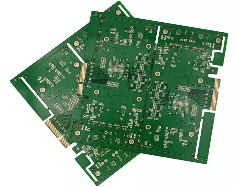
High frequency PCB design is never a simple combination of individual rules. It is a systematic engineering process that requires continuous trade-offs among electromagnetic compatibility (EMC), signal integrity, and manufacturing cost. Modern high-frequency electronic devices generally feature high integration density and compact component placement. Single-layer or double-layer PCBs often struggle to meet both routing and noise-immunity requirements, making multilayer boards an inevitable choice for high-frequency circuits.
Proper planning of the layer count and board dimensions allows the inner layers of the PCB stackup to be used effectively as electromagnetic shielding barriers. This not only facilitates short, direct grounding paths for components but also reduces parasitic inductance and shortens signal propagation paths. Measured data shows that, when the same PCB material is used, a four-layer board can provide approximately 20 dB better noise suppression than a double-sided board, while significantly reducing crosstalk.
However, increasing the number of layers also increases manufacturing complexity and hardware costs. Therefore, designers must determine the appropriate layer count based on the actual functional requirements of the circuit and continuously optimize component placement and routing rules to achieve the best balance between the performance ceiling and cost constraints of a high frequency PCB.
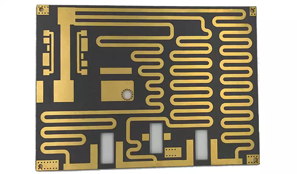
Routing geometry is the first practical expression of high frequency PCB design principles. Traces should preferably be routed in straight lines. When layout constraints require a change in direction, 45-degree bends or curved transitions should be used, while 90-degree corners should be strictly avoided. Although such practices in low-frequency circuits may primarily help improve the mechanical connection between copper traces and the substrate, under high-frequency operating conditions, they can reduce signal radiation and electromagnetic coupling between adjacent traces, thereby suppressing interference at its source.
At the same time, the radiation intensity of high-frequency signals is directly related to trace length. The longer the trace, the more significant the radiation effect and the greater the possibility of coupling interference with surrounding components and adjacent traces, which can eventually lead to signal distortion and data transmission errors. Therefore, high-frequency and high-speed signal traces, including clock lines, crystal oscillator traces, DDR data buses, LVDS, USB, and HDMI, should follow the principle of keeping the routing path as short as possible to minimize signal propagation distance.
While shortening trace lengths, designers should also minimize signal layer transitions. The key is to strictly control the number of vias. A typical through via can introduce approximately 0.5 pF of parasitic capacitance. This parasitic capacitance can degrade high-frequency signal transmission performance and increase the probability of data errors. Therefore, minimizing vias and reducing unnecessary layer transitions is one of the most straightforward and effective ways to improve the operating speed and signal integrity of a high frequency PCB.
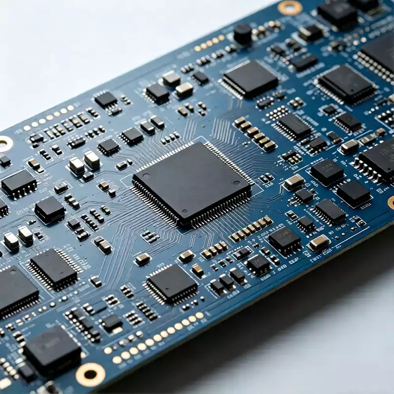
Crosstalk caused by parallel routing is another common issue that must be carefully controlled in high frequency PCB design. Crosstalk refers to unwanted noise interference generated through electromagnetic coupling between two signal traces that have no direct electrical connection. High-frequency signals propagate along PCB traces in the form of electromagnetic waves, and each signal trace can effectively act as a miniature transmitting antenna that radiates an electromagnetic field. When the electromagnetic fields of adjacent traces overlap and couple with each other, additional noise is generated. The PCB stackup, trace spacing, electrical characteristics of the driver and receiver, and termination method all affect crosstalk to varying degrees. These parameters must therefore be optimized individually during the design process.
Power integrity is another major source of interference. To effectively suppress high-frequency harmonic noise on power pins, a high-frequency bypass or decoupling capacitor should be placed as close as possible to the power pin of each integrated circuit. This allows high-frequency noise on the power rail to be filtered rapidly, preventing harmonic noise from propagating through the power distribution network and across the entire PCB, thereby maintaining clean and stable power delivery to the IC.
Grounding is equally important. Proper isolation between analog ground and digital ground must be carefully considered because the ground potential of high-frequency digital circuits is constantly fluctuating and contains substantial high-frequency harmonic components. If digital ground and analog ground are directly interconnected without proper consideration, these harmonics can couple through the ground network into analog signal paths, seriously affecting sampling accuracy and stability. In practical engineering, a single-point grounding scheme is commonly used for controlled interconnection between the two ground domains, or a high-frequency ferrite bead can be used to connect them. These approaches help block unwanted noise propagation and minimize interference between analog and digital signal domains.
Signal reflection is another issue that cannot be overlooked. When a high-frequency signal encounters an impedance discontinuity along its transmission path, signal reflections occur, causing overshoot, ringing, and waveform distortion. The voltage level may repeatedly oscillate around the logic threshold, eventually resulting in logic errors and abnormal system operation. The key to solving this problem is to achieve accurate impedance matching between the transmission line and the load.
The closer the load impedance is to the characteristic impedance of the transmission line, the smaller the reflection amplitude and the better the signal integrity. Therefore, high frequency PCB design must maintain continuous controlled impedance throughout the entire transmission path. Sudden changes in trace width, sharp bends, and other discontinuities should be avoided to prevent local impedance mismatches from causing signal reflections and distortion.
Based on the core design principles of EMI control, impedance matching, and signal integrity, the industry has established standardized routing guidelines for various high-speed and high-frequency interfaces. USB differential pairs should use symmetrical differential routing throughout the entire signal path, with a trace width of 10 mil, an intra-pair spacing of 6 mil, and a 6 mil clearance between the traces and the ground. HDMI differential pairs should likewise use a symmetrical structure, with a single-trace width of 10 mil and an intra-pair spacing of 6 mil, while the spacing between differential pairs should be greater than 20 mil.
LVDS differential traces should use a 7 mil trace width and a 6 mil intra-pair spacing, with differential impedance controlled precisely within 100 Ω ±15%. For DDR1 signals, routing should preferably remain on the outer layer throughout the signal path to minimize vias. All signal traces should maintain consistent trace width and spacing and follow the 2W routing rule. For DDR2 and higher-speed memory interfaces, all high-frequency data traces should also be length-matched and impedance-controlled to ensure synchronized high-speed data transmission and prevent timing skew.
High frequency PCB design ultimately revolves around three fundamental pillars: EMI control, impedance matching, and signal integrity. By strictly following appropriate routing practices, grounding strategies, and interface-specific design standards while balancing layout efficiency and manufacturing cost, designers can effectively prevent common problems such as signal distortion, crosstalk, and reflections. This provides a solid foundation for the long-term stability, reliability, and performance of high-frequency electronic systems.