High frequency PCBs for military radar serve as the core hardware platform within radar systems, undertaking critical tasks such as signal transmission, power amplification and processing; their performance directly determines the radar’s detection accuracy, anti-jamming capability and response speed. As military radars typically operate in the microwave to millimetre-wave bands (40–94 GHz), high frequency signals are highly susceptible to issues such as signal loss, impedance mismatch and electromagnetic interference during transmission. Even the slightest design deviation can lead to signal distortion, reduced detection range or even system failure.
Compared to civilian high frequency PCBs, military radar high frequency PCBs must not only ensure signal integrity but also meet reliability challenges in extreme environments. Consequently, the design must balance signal transmission efficiency, structural stability and environmental adaptability, achieving systematic breakthroughs in both technology and manufacturing processes.
High-quality design is not merely a matter of stacking parameters, but rather a systematic engineering process that integrates materials science, electromagnetic theory and process technology, based on radar operational requirements. From substrate selection and laminate structure to routing optimisation and impedance control, every stage requires precise calculation and repeated verification to ensure the PCB operates stably in complex battlefield environments, thereby supporting the upgrade of defence equipment towards high precision, intelligence and miniaturisation.
Selection of Base Materials
The base material serves as the substrate for high frequency PCBs; the stability of its dielectric constant (Dk) and the magnitude of its loss tangent (Df) directly affect signal loss and phase consistency. Furthermore, military radar systems must withstand extreme conditions such as high temperatures, vibration and humidity; therefore, the base material must possess low water absorption, high toughness and a suitable coefficient of thermal expansion (CTE).
Current mainstream choices include specialised high frequency materials such as RO5880 and Rogers 4350B. Taking RO5880 as an example, with Dk = 2.20 ± 0.02 and Df = 0.0009 at 10 GHz, it effectively reduces dielectric loss and ensures low-distortion signal transmission. Its CTE is highly compatible with that of metal conductors, reducing the risk of interlayer warping and delamination caused by temperature fluctuations. Furthermore, the substrate must possess high mechanical strength and low water absorption (≤0.04%) to prevent a decline in dielectric properties due to moisture penetration and to withstand harsh environments involving strong vibrations and impacts.
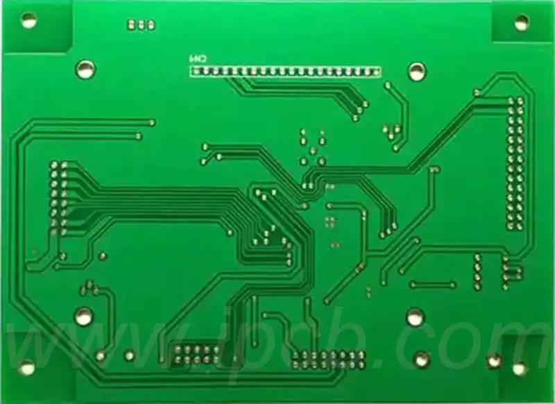
Layer Stack-up and Routing Optimisation
Scientific layer stack-up and routing design are key to addressing signal integrity and electromagnetic compatibility (EMC). High-frequency signals are prone to crosstalk, reflections and insertion loss, whilst demands for high-density miniaturisation further increase routing complexity.
The layer stack-up design should adopt an alternating ‘signal layer–ground layer’ structure, utilising continuous copper foil planes to create a shielding effect, suppress external interference and provide a low-impedance return path for high-frequency signals. For multilayer boards (typically 8–16 layers), the spacing between power planes and signal layers must be carefully planned to enhance coupling and minimise crosstalk and power supply noise coupling.
Routing principles emphasise “short, straight, and uniform”: signal traces should be kept as short as possible, avoiding meandering; corners should be routed at 45° or with rounded curves to prevent the impedance spikes caused by right angles. Differential signals (such as transmit and receive signals) must be routed in parallel at equal distances, with length differences controlled within 5 mils, and spacing adhering to the 3W rule (line spacing ≥ 3 times the line width) to minimise crosstalk.
Via optimisation is a critical detail: use blind or buried vias, or back-drilling techniques to remove stubs, thereby reducing parasitic capacitance and resonance losses. Ground vias should be placed adjacent to signal vias (spacing ≤ 0.5 mm) to form a shielding structure. For millimetre-wave radar, via diameters should be controlled between 0.3–0.4 mm to ensure stable transmission.
Impedance Control
Impedance matching directly affects signal integrity and detection performance. Impedance deviations exceeding ±5% can cause reflections, leading to excessive echo loss and signal distortion. Therefore, impedance control must be integrated throughout the entire design and manufacturing process.
RF signals typically employ a 50 Ω single-ended impedance (e.g., antenna feedlines, power amplifier outputs), with a precision requirement of ±3% and return loss ≤ -15 dB at 10 GHz; millimetre-wave signals, however, require high precision of ±2% and commonly use 75 Ω or 100 Ω impedance. During design, parameters such as the substrate’s Dk, trace width, trace spacing and dielectric thickness must be taken into account, with precise calculations performed using specialist software to ensure the smallest possible deviation between design values and actual manufacturing results.
Environmental Adaptability Design
Military radar is frequently deployed on aerospace, shipborne and vehicle-mounted platforms, facing challenges such as high and low temperatures, severe vibration, strong electromagnetic interference and high humidity; environmental adaptability is a core differentiating requirement in design.
Vibration and Shock Resistance: Structurally, reinforced borders are incorporated around the PCB board edges, and high-mass components (such as power amplifiers) are positioned near the centre to reduce stress concentration. In terms of manufacturing processes, lead-free solder and reinforced solder mask layers are used to enhance joint strength; during lamination, the copper foil thickness is increased (≥2 oz) to improve mechanical toughness and resistance to delamination.
Electromagnetic Compatibility (EMC): Separate ground and power planes are established, with multi-point grounding (ground via spacing ≤ 5 mm); ground vias are arranged on both sides of high-frequency signal lines to form a ‘shielding wall’; power plane segmentation is optimised to avoid overlap between high-frequency and digital power supplies, and ferrite beads are used to isolate noise. In high-interference environments, a metal shielding enclosure may be installed.
High-temperature resistance and moisture protection: Select high-temperature-resistant substrates and solder mask layers to support an operating range of -55°C to 125°C. Substrate pre-treatment must thoroughly remove moisture and oil contamination to minimise interlayer voids. Apply silver or gold plating to the surface to enhance corrosion resistance and moisture protection, ensuring long-term reliability in high-humidity and salt-fog environments.
The design of high frequency PCBs for military radar is a multidisciplinary systems engineering project. Every detail, from materials to processes, must be refined to the highest standards to provide a robust and reliable hardware foundation for the radar system.