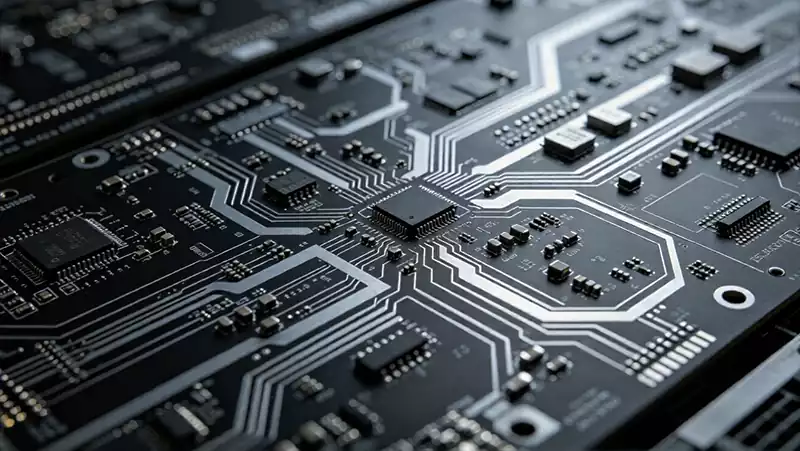
In the field of PCB manufacturing, the circuit patterning process is a critical factor in determining the performance and quality of the PCB. Among these, Tenting (subtractive process), SAP (semi-additive process) and mSAP (modified semi-additive process) are three core processes, each with its own unique characteristics and suitable applications. These three processes differ significantly in terms of starting materials and circuit formation methods, resulting in distinct advantages and limitations regarding precision, cost and suitability. Below, we provide a detailed introduction to these three processes.
Tenting (Conventional Subtractive Process): The Widespread Application of a Mature Process
Tenting, also known as the conventional subtractive process, is arguably the ‘pioneer’ of PCB manufacturing processes; it is the most traditional and widely used method. Its core principle can be summarised as ‘complete coverage, selective removal’, whereby a series of operations removes the unwanted copper layers, thereby retaining the required circuits.
Process Flow
Substrate Preparation: A copper-clad laminate (CCL) coated with a thick layer of copper foil (typically ≥12μm) is selected as the starting material. The thick copper foil provides the foundation for subsequent etching operations.
Pattern Transfer: A dry film is applied to the surface of the copper foil. Using exposure and development techniques, the circuit pattern is precisely transferred onto the dry film. At this stage, the areas of the circuit to be retained are protected by the dry film, as if these areas were clad in a layer of ‘protective armour’.
Etching: The copper foil is etched using a chemical etching solution. During this process, all copper not protected by the dry film is etched away, leaving only the circuit sections protected by the dry film.
Stripping: The dry film is removed, resulting in a clear circuit pattern.
Advantages
Mature and stable process: After years of development and practical application, the tenting process has become highly mature. The workflow is straightforward and easy to understand, and the equipment investment is relatively low. During mass production, it maintains a high level of stability and achieves a respectable yield rate.
Low cost: Due to its simplicity and modest equipment requirements, production costs are relatively low. Consequently, it is highly suitable for the mass production of standard PCBs and meets the cost-control requirements of sectors such as consumer electronics.
Controllable copper thickness: The copper thickness can be adjusted according to specific requirements, ranging from 12 to 40 μm. This provides a unique advantage in industrial-grade applications requiring high current transmission, as it can withstand significant current loads.
Disadvantages
Severe side etching: During the etching process, due to the characteristics of the chemical etching solution, side etching occurs, resulting in trapezoidal-shaped traces. This shape affects the impedance consistency of the traces, thereby impacting the electrical performance of the PCB.
Limited line width/spacing: It is difficult to produce ultra-fine traces; typically, the limit for line width/spacing (L/S) is around 30μm/30μm. As the demand for miniaturisation and high integration in electronic devices continues to rise, this limitation is becoming increasingly apparent.
High consumption of etching solution and significant pollution: The etching process requires a large amount of chemical etching solution and generates a considerable amount of pollutants, placing a certain burden on the environment.
Main Application Scenarios
The Tenting process is primarily used in scenarios where line width requirements are not particularly stringent, such as standard PCBs and consumer electronics motherboards. These products are cost-sensitive and have relatively low requirements for circuit precision; the tenting process is well-suited to meeting their production needs.
SAP (Semi-Additive Process): Pursuing the Ultimate in Circuit Precision
The SAP process was developed to meet the demands of applications requiring the highest level of circuit precision. Its core lies in the combination of a ‘thin copper seed layer + selective electroplating + flash etching’, enabling the fabrication of ultra-fine circuits through unique process steps.
Process Flow
Preparation of Copper-Free Substrates: Starting with bare dielectric materials (such as ABF film) that lack copper foil, a clean surface is provided for subsequent seed copper deposition.
Seed Copper Deposition: Using chemical deposition methods, an extremely thin (<1μm) “seed layer” of copper is formed across the entire dielectric surface. This seed copper acts like individual “seeds”, providing the foundation for subsequent electroplating growth.
Pattern Transfer: A dry film is applied; following exposure and development, the areas where the circuit lines are to be formed are exposed. At this stage, the dry film acts as a mask, protecting the areas that are not to be electroplated.
Pattern Electroplating: The exposed seed layer is electroplated to increase its thickness to the design specification. Through the electroplating process, copper is gradually deposited onto the seed layer, forming the required circuit line shapes.
Stripping + Flash Etching: After removing the dry film, a rapid ‘flash etching’ process is used to etch away the extremely thin seed layer not covered by the deposited copper. This yields the final circuit pattern.
Advantages
Ultra-fine line widths and spacings: As the seed layer is extremely thin, the etching process has minimal impact on it, enabling ultra-fine line widths and spacings of 10μm to 20μm. These ultra-fine circuits meet the high integration requirements of high-end electronic devices, providing strong support for the miniaturisation and high performance of chips.
High circuit precision and good impedance consistency: Minimal side etching and a near-rectangular cross-section significantly improve the impedance consistency of the circuits. This is crucial for PCBs used in high-speed signal transmission, as it reduces signal distortion and interference, thereby enhancing circuit performance.
Disadvantages
Complex process and high costs: The SAP process involves a lengthy workflow comprising multiple complex steps, with very high demands on equipment and materials. This not only increases production costs but also makes process control more difficult.
Stringent requirements for the seed layer: The uniformity and adhesion of the seed layer have a crucial impact on the final line quality. Ensuring consistent seed layer quality requires strict control of chemical deposition process parameters, which poses a significant challenge for yield management during production.
Limited production capacity: Due to its complexity and relatively long production cycle, production capacity is lower than that of the Tenting process. Consequently, it is unsuitable for the production of low-cost products.
Main application scenarios
The SAP process is primarily used in high-end server CPU/GPU packaging and IC substrate applications requiring ultra-high-density interconnects. These fields demand extremely high precision and performance from circuit lines, and the SAP process meets their requirements for ultra-fine lines and excellent electrical performance.
mSAP (Modified Semi-Additive Process): The mainstream choice for high-end applications
The mSAP process is currently the mainstream technology for high-end applications. It strikes an excellent balance between cost and performance, combining the key advantages of both the Tenting and SAP processes. Its core principle is ‘thin base layer with selective thickening’.
Process Flow
Substrate Preparation: A copper-clad laminate with ultra-thin copper foil (typically 1–3 μm) is selected, or a thin copper layer is deposited directly onto the dielectric as a “seed layer”. This ultra-thin copper layer provides the foundation for subsequent selective thickening.
Pattern Transfer: A photoresist film is applied; following exposure and development, the areas where circuits are to be formed are exposed. Similar to the SAP process, the photoresist acts as a mask.
Pattern Electroplating: Patterned electroplating is performed on the exposed thin copper layer to thicken it to the required design thickness. The electroplating process achieves both the thickening and shaping of the circuit lines.
Stripping + Flash Etching: After removing the dry film, a “flash etching” process is used to rapidly remove the original thin copper layer. This yields the final circuit pattern.
Advantages
High circuit precision: Effectively overcomes the side etching issues associated with the tenting process; the circuit cross-section is approximately rectangular, and impedance control is optimised. This makes it highly suitable for high-frequency/high-speed (5G, optical modules) applications, meeting the stringent requirements for signal transmission quality in these fields. Additionally, line widths and spacings of 15–25 μm can be achieved, further enhancing circuit integration.
Balance of cost and performance: Compared to the SAP process, the mSAP process is more cost-effective; whilst compared to the Tenting process, it offers higher precision. In high-end applications, it effectively controls production costs whilst ensuring performance, offering excellent value for money.
Disadvantages
Complex process and higher costs: Although simplified compared to the SAP process, the mSAP process still involves more steps than the Tenting process and places higher demands on equipment and materials. This results in relatively high production costs, which to some extent limits its scope of application.
Slightly lower precision than SAP: During the flash etching process, there is still a slight impact on line precision, and its theoretical limit is lower than that of the SAP process. For certain extreme application scenarios with extremely high requirements for circuit precision, it may not fully meet the demands.
Main Application Scenarios
The mSAP process is primarily used in high-end mobile phones, AI accelerator cards, and SLP (Small Land Pattern) applications. These sectors place high demands on PCB performance and integration, whilst also requiring a degree of cost control. As the mSAP process can meet performance requirements whilst offering relatively reasonable costs, it has become the preferred process in these fields.
In summary, the Tenting, SAP and mSAP processes each have their own advantages and disadvantages and are suitable for different application scenarios. In actual production, the appropriate process for PCB fabrication must be selected based on factors such as specific product requirements, cost budgets and production scale, in order to achieve the optimal balance between performance and cost. With the continuous development of electronic technology, these three processes will also continue to be improved and refined, providing stronger support for the development of the PCB industry.