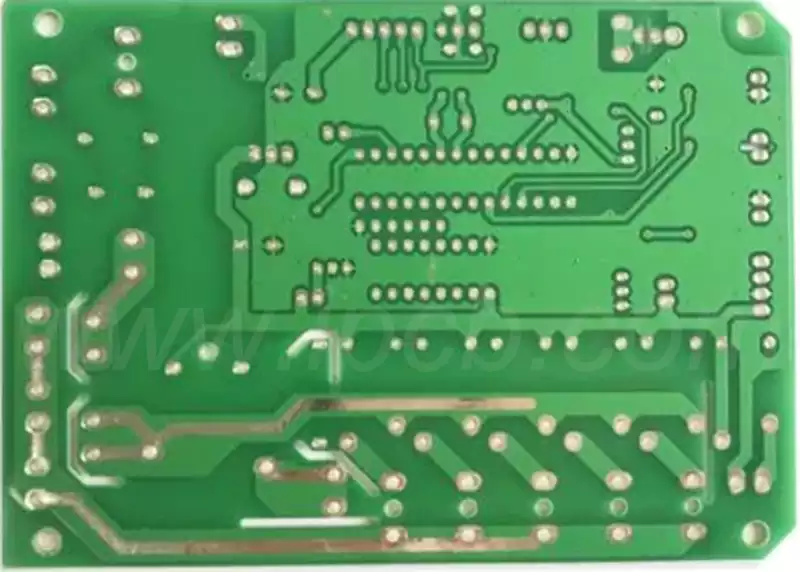
A single sided PCB board is one of the simplest forms of printed circuit board construction, using only one copper layer to create the conductive pattern. Unlike a double-sided or multilayer PCB, the electrical connections on a single-sided board must be routed through the same conductive layer. This limits routing flexibility, but it also gives the board a relatively simple structure that can be useful for products with low circuit density and straightforward electrical requirements.
The decision to use a single sided PCB board should not be based only on manufacturing cost. Board size, component placement, current requirements, thermal conditions, assembly processes, and routing complexity all affect whether a one-layer structure is practical. When these factors are compatible with a single conductive layer, the simpler construction can provide an efficient solution for high-volume electronic products.
A single sided PCB board has one conductive copper layer laminated to an insulating substrate. The copper is patterned during PCB fabrication to form traces, pads, and other conductive features required by the circuit. Components are normally mounted on the opposite side or positioned so that their terminals connect to the copper pattern through drilled holes, depending on the board construction and assembly method.
The main characteristic of this structure is the absence of a second copper routing layer. On a double-sided PCB, a signal can move between the top and bottom copper layers through vias or plated through-holes. A single sided PCB board does not provide the same routing option, so all traces must be arranged on one conductive surface.
This difference has a direct effect on PCB layout. Two independent traces cannot simply cross each other on the same copper layer. If the schematic requires connections that would normally intersect, the designer has to change the component placement, find another routing path, or introduce an electrical jumper where appropriate. When the number of such crossings becomes too high, the design may be better suited to a double-sided PCB.
IPC recognizes single-sided rigid printed boards as a distinct PCB construction and includes them within the scope of rigid printed board performance requirements. The exact construction and acceptance requirements depend on the applicable specification and the intended application.
How the Structure Affects single sided PCB board Design
The simplicity of a single sided PCB board changes the way the circuit should be laid out. On a multilayer board, the designer can use different layers for signal routing, power distribution, and ground planes. On a single-sided board, these functions have to be accommodated within the same copper pattern.
Component placement therefore becomes one of the most important parts of the design process. Components should be positioned according to their electrical relationships rather than simply arranged to make the board look symmetrical. Devices belonging to the same circuit section can often be placed closer together so that their connections can be routed without unnecessary crossings.
Power paths require particular attention. High-current traces should be designed with sufficient conductor width and copper thickness for the expected current and allowable temperature rise. A narrow trace may be electrically functional under normal conditions but still create excessive resistance or localized heating when carrying higher current. Trace width should therefore be calculated according to the electrical requirements and applicable PCB design rules rather than selected from a generic value.
The same principle applies to clearance. Required spacing depends on factors such as operating voltage, environmental conditions, manufacturing capability, and the applicable safety or design standard. There is no single clearance value that is appropriate for every single sided PCB board.
For relatively simple circuits, the routing process can be straightforward. As component density increases, however, the lack of a second copper layer becomes increasingly important. A design may still be technically routable, but excessive detours and jumpers can increase board area, complicate assembly, and make troubleshooting more difficult.
Materials and Construction
The substrate used for a single sided PCB board depends on the electrical, mechanical, thermal, and cost requirements of the application. FR-4 is widely used for rigid printed circuit boards because of its combination of mechanical strength, electrical insulation, thermal performance, and dimensional stability. Other laminate systems can also be used when a product requires different material characteristics.
Copper thickness is another important construction parameter. The copper layer must provide adequate conductivity for the circuit while also meeting the requirements of the manufacturing process. Standard copper thickness may be sufficient for many low-current circuits, while power-oriented applications may require heavier copper or wider conductors.
The final board can also include solder mask, silkscreen, and a surface finish. The selected surface finish depends on the component technology, soldering process, storage requirements, and reliability expectations. HASL, lead-free HASL, OSP, and ENIG are examples of finishes used in PCB manufacturing, although the appropriate option depends on the specific product requirements.
These construction parameters should be defined as part of the PCB fabrication specification. Treating a particular material, copper thickness, trace width, or surface finish as a universal requirement can lead to an unsuitable design because PCB requirements vary considerably between applications.
Manufacturing Process of a Single Sided PCB Board
The manufacturing process for a single sided PCB board is generally less complex than that of a multilayer PCB because only one conductive layer needs to be patterned. Even so, each manufacturing stage affects the quality of the finished circuit.
Production begins with the preparation of the copper-clad substrate. The required circuit pattern is then transferred to the copper surface using the selected imaging process. During etching, unwanted copper is removed so that the required traces and pads remain.
After the circuit pattern has been formed, holes can be drilled or punched according to the design. These holes may be used for through-hole components, mounting hardware, or other mechanical requirements. The board then goes through solder-mask and marking processes when these features are included in the specification.
A surface finish is applied to exposed copper areas when required. The finished boards are subsequently inspected and electrically tested to identify issues such as opens and shorts. Dimensional inspection and visual inspection may also be performed to verify that the finished board conforms to the production requirements.
Although the process itself is relatively straightforward, manufacturing capability still has to be considered during PCB design. Minimum trace width, minimum spacing, hole diameter, annular ring, board thickness, copper thickness, and other parameters should be compatible with the fabrication process selected for production.
Where Single Sided PCB Boards Are Used
The practical applications of single-sided construction are closely related to its routing limitations. Products with relatively simple circuits and moderate component density can often take advantage of the structure without requiring the additional routing flexibility of a double-sided PCB.
Simple LED control circuits are one example. Many LED products contain relatively straightforward electrical connections and can accommodate a single conductive layer when sufficient board area is available. Basic power circuits and low-complexity control boards can also use single-sided construction when the current paths and component placement can be arranged effectively.
Some household appliances and industrial control products contain relatively simple electronic circuits that do not require high-density routing. In these cases, a single sided PCB board can provide an appropriate balance between circuit functionality and manufacturing complexity.
The suitability of the board should still be evaluated at the individual circuit level. The fact that a product belongs to a particular application category does not automatically mean that a single sided PCB board is the correct choice. A compact appliance controller with many components, for example, may require a double-sided or multilayer structure even though another controller in the same product category could use a single layer.

Single Sided PCB Board Advantages and Limitations
The main advantage of a single sided PCB board is its relatively simple construction. With only one conductive layer, the fabrication process does not require the additional lamination and interconnection structures associated with multilayer boards. This can make the board attractive for cost-sensitive products, particularly when the design is produced in large quantities.
The simple structure can also make visual inspection and circuit tracing easier. When the circuit pattern is concentrated on one conductive surface, technicians can often follow the electrical connections without having to interpret multiple copper layers.
However, these advantages come with a fundamental limitation: routing density. A single copper layer provides fewer options for connecting a large number of components. Once the circuit becomes dense, the designer may need to use longer traces, larger board dimensions, jumpers, or alternative component arrangements to complete the routing.
This limitation can affect more than the PCB layout itself. Additional jumpers may introduce extra assembly operations. A larger board can increase enclosure size. Longer traces can influence electrical performance. Limited copper area can also make power distribution and thermal management more difficult.
For this reason, the lowest PCB layer count does not always produce the lowest overall product cost. The complete manufacturing and assembly process should be considered before deciding on the board structure.
Single Sided PCB board vs Double Sided PCB
The difference between a single-sided and double-sided PCB is primarily the number of available conductive layers, but the practical impact extends to almost every aspect of PCB layout.
A single sided PCB provides one copper layer, which limits routing flexibility but keeps the construction relatively simple. A double-sided PCB provides conductive copper on both sides, allowing signals and power connections to be distributed between layers. Vias and plated through-holes can be used to establish electrical connections between the two sides.
This additional routing flexibility makes double-sided construction more suitable for circuits with higher component density or more complicated interconnections. It can also allow the same circuit to occupy a smaller board area.
The choice should therefore be made according to the actual design requirements. If a circuit can be routed cleanly on one copper layer while maintaining suitable electrical clearances, current capacity, thermal performance, and assembly requirements, a single-sided board may be sufficient. If routing requires numerous jumpers or the board must be substantially smaller, moving to a double-sided structure may provide a better engineering solution.
When a Single Sided PCB board Is No Longer Practical
A single-sided architecture becomes less attractive when routing complexity begins to create secondary design problems. A high jumper count is one useful warning sign. If jumpers are being added repeatedly simply to overcome trace crossings, the circuit may already be beyond the practical routing capability of a single copper layer.
Component density is another consideration. As packages become smaller and the number of electrical connections increases, the available routing area becomes increasingly difficult to manage. A larger PCB can solve part of this problem, but the additional board area may conflict with the mechanical requirements of the final product.
Electrical performance can also determine the layer structure. High-speed circuits often require careful control of signal return paths, impedance, coupling, and loop area. A single-sided architecture may not provide sufficient flexibility to establish the required routing and reference structures.
Thermal requirements should also be evaluated. Power components and high-current paths may need substantial copper area for current carrying and heat spreading. If the available copper pattern cannot provide the required thermal or electrical performance, a different PCB construction may be more appropriate.
Designing a Reliable Single Sided PCB Board
A reliable single sided PCB board begins with an appropriate circuit architecture. Before routing starts, the designer should understand which connections are critical, which components have fixed mechanical positions, where high-current paths will run, and which areas require electrical isolation.
The schematic should be translated into a physical arrangement that minimizes unnecessary crossings. Components should be placed with their electrical relationships in mind, and the most important signal and power paths should be considered before less critical connections.
The design should then be checked against the intended manufacturing process. Trace width and spacing need to satisfy the electrical requirements while remaining within the fabricator’s process capability. Hole sizes, annular rings, board thickness, copper thickness, and surface finish should also be defined clearly in the fabrication documentation.
Testing should be considered before the layout is finalized. Appropriate test points can make production testing and troubleshooting easier, particularly when the PCB will be manufactured in large quantities.
The most effective single-sided designs are not simply boards that happen to contain one copper layer. They are designs in which the circuit topology, component placement, routing strategy, manufacturing process, and assembly method have all been considered together.
A single sided PCB board remains a practical option for electronic products that can be routed effectively on one conductive layer. Its simple construction can reduce manufacturing complexity and provide cost advantages for suitable applications, but those advantages depend on keeping circuit density and routing requirements within reasonable limits.
The most important consideration is therefore not whether a single sided PCB board is cheaper than a double-sided or multilayer board in isolation. The better question is whether the one-layer structure can satisfy the complete product requirements without creating excessive jumpers, board area, assembly work, thermal constraints, or electrical limitations.
For simple and low-density circuits, a single sided PCB board can be an efficient and reliable solution. As routing density, miniaturization, signal speed, power requirements, or thermal demands increase, a double-sided or multilayer construction may become more appropriate.