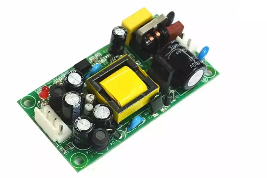
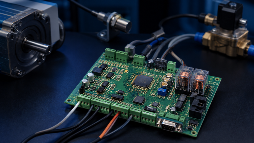
A PCB main board can operate successfully on an engineer’s bench and still be unprepared for production. Prototype technicians can replace components, add jumper wires and adjust firmware until one board works, but a factory must reproduce the same result across every unit without depending on manual correction.
The move from prototype to production exposes weaknesses in a PCB main board that may not appear during basic functional testing. Power sequencing can become unstable when component tolerances change. High-speed interfaces may work on one sample but fail at temperature. A BGA joint can pass visual inspection while remaining marginal, and incomplete test access can allow assembly defects to reach final product integration. Successful production therefore depends on converting prototype knowledge into controlled design data, measurable electrical limits and repeatable test procedures before the manufacturing volume increases.
The main board is the primary circuit assembly that connects the processor, memory, power supplies and major input and output interfaces of an electronic product. It may also carry communication devices, storage, sensor interfaces, audio circuits, displays or motor-control connections. What separates the PCB main board from a peripheral or interface board is its system-level responsibility. A fault in a peripheral board may disable one feature, while a problem in the main board can prevent the entire product from starting, communicating or completing its intended function. This concentration of functions creates conflicting layout requirements. The processor and memory need short, controlled high-speed connections. Switching regulators require compact high-current loops. Analogue circuits need protection from noise, while external connectors require ESD or surge protection. Mechanical constraints may also force large connectors and heat-generating devices into limited board space. A production-ready design must preserve all these relationships while remaining possible to fabricate, assemble, inspect and test consistently.
Manufacturing a PCB main board requires more than sending Gerber files and a component list. The production package must define one internally consistent hardware revision. The Gerber or ODB++ data, drill files, stack-up, controlled-impedance requirements, BOM, centroid file, assembly drawing, schematic, programming file and test specification must all describe the same version. If one file is revised independently, the manufacturer may build a board that is mechanically correct but electrically incompatible with the intended firmware or component set. Component designations should be consistent across the schematic, BOM, placement file and assembly drawing. Manufacturer part numbers are preferable to generic descriptions such as “10 µF capacitor” because package size, voltage rating, dielectric material and DC-bias behavior can all affect performance. Do-not-populate components also need explicit control. Pads for debugging options, alternative boot configurations or unused interfaces may remain in the design, but the production documentation must clearly identify which parts are fitted for each product version. Formal schematic review before layout release reduces problems during board bring-up. TI recommends reviewing processor power, clocks, reset, boot configuration, DDR, storage and communication interfaces before progressing through layout and testing. The purpose of data control is not administrative neatness. It prevents the factory from combining correct files that belong to different product revisions.
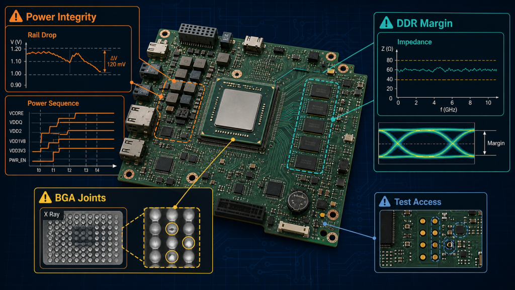
Processor-based main boards usually contain several supply rails. The processor core, I/O banks, memory, analogue circuits and communication devices may require different voltages, current capacities and startup sequences. On a PCB main board, correct voltage measured at the regulator does not guarantee correct voltage at the processor. Copper resistance, via transitions and transient current can produce a voltage drop between the source and the load. Critical rails should therefore be measured near processor or memory decoupling capacitors, not only at the regulator output. Power-up and power-down behavior also matter. An I/O signal driven before its receiving power domain becomes valid may create unintended current paths or unreliable boot behavior. Pull-up resistors must reference the appropriate supply, and external devices should not drive non-fail-safe processor pins before their I/O rail is available. NXP’s board bring-up guidance recommends visually checking component orientation before power is applied and verifying critical rails close to the processor to reveal board-level voltage drop. Prototype validation should include supply ramp, reset release, clock startup and worst-case load transitions. Production testing does not need to reproduce every engineering measurement, but the design must provide accessible points for critical rails, reset and boot status. Power integrity problems are expensive after production begins because they often appear intermittent. A unit may pass initial testing and then reset during processor load, peripheral startup or a temperature change.
DDR, eMMC, USB, Ethernet, display links and high-speed expansion interfaces depend on trace geometry, reference planes, length relationships and return-path continuity. Passing data on a single prototype does not establish sufficient production margin. Variations in laminate properties, copper thickness, etching and assembly parasitics can move a marginal interface from working to failing. Controlled impedance should therefore be defined with the PCB manufacturer’s actual stack-up rather than copied from a generic calculator. The routing of high-speed interfaces on the PCB main board should minimize discontinuities, crosstalk and unnecessary via stubs. Clock and strobe signals require particular attention because disturbances on these nets can affect the timing of an entire data group. TI’s processor-board guidance recommends considering via coupling, via stubs, propagation delay and signal-integrity simulation for interfaces such as eMMC, SDIO, OSPI, QSPI and RGMII. Validation should exercise interfaces at their intended speed and under realistic data traffic. Detecting a USB connector or memory device is not equivalent to verifying sustained operation. Storage tests should read and write substantial data, network interfaces should run traffic, and memory should be stressed with patterns capable of revealing timing or data-line errors.
Processors, memories and high-density interface devices often use BGA packages. Their solder joints are hidden beneath the component, so conventional optical inspection cannot directly confirm joint shape, voiding or bridging. The assembly yield of a PCB main board depends on land-pattern accuracy, solder-paste deposition, package warpage, moisture handling and a reflow profile suitable for both the BGA and the surrounding components. A profile developed around only the largest component may overheat smaller parts, while insufficient thermal input can leave hidden joints incompletely formed. X-ray inspection is useful for identifying bridging, missing solder, major voiding and alignment problems beneath BGA packages. It should be applied according to package risk and process validation rather than treated as a substitute for controlling printing and reflow. Test coverage remains necessary because an X-ray image cannot prove that every connection is electrically reliable. Boundary scan, processor diagnostics or functional interface testing may be needed where physical probe access is limited. Panel support and depanelization also deserve attention. Large, thin or asymmetrically populated boards can bend during assembly or separation. Mechanical strain near a BGA can damage otherwise acceptable joints, particularly when a connector or mounting hole is positioned close to the package.
A board that displays a boot logo has demonstrated only a small part of its function. Production testing must verify the PCB main board through the interfaces and operating states most likely to reveal assembly faults. Initial checks should confirm shorts, input current and the principal supply rails before full power is applied. The next stage can verify processor boot, programmed firmware, memory, storage and essential communication interfaces. Product-specific tests then exercise displays, sensors, audio, network ports, motors or other peripherals. TI notes that board diagnostic software is useful for verifying interface continuity and assembly, but it does not replace complete product software or application-level testing. Design for test should begin before layout completion. Test points need adequate size and spacing, but they must not create stubs on sensitive high-speed signals. Where direct probing is unsuitable, firmware diagnostics, boundary scan or connector-based fixtures may provide better coverage. The test record should identify the hardware revision, firmware version and test result for each serial number or production batch. Without this link, a later field problem cannot be reliably associated with a specific component lot, assembly process or software release.
Changes are normal during the transition to production. A component may become unavailable, a connector may move or firmware may require a different boot configuration. The risk comes from allowing a change to enter production without updating every dependent document. When any change reaches a PCB main board, its effect should be reviewed across the schematic, layout, BOM, assembly program, inspection program, firmware and functional test. Even a nominally equivalent component can have different pin behavior, startup timing, thermal performance or package dimensions. A controlled engineering-change process should identify the first production batch that uses the new revision. Remaining material from the previous version must be separated, and mixed-revision rework needs documented instructions. Prototype modifications made with jumper wires also require a clear decision. They must either be incorporated into the production layout or removed after the underlying issue is resolved. An undocumented jumper should never become a permanent production instruction.
Design for manufacturing evaluates whether the board can be fabricated and assembled consistently. Design for assembly examines component spacing, orientation, process sequence and mechanical access. Design for test ensures that faults can be detected before the board reaches final product integration. These reviews are most valuable before tooling is released. Moving a component or adding a test point is inexpensive during layout, but the same change becomes costly after stencils, fixtures and production documentation have been completed. IPC describes DFM, DFA and DFT as connected design practices that improve manufacturability, assembly and testability rather than as separate checks performed after the design is finished. The review should focus on the actual manufacturer’s capabilities. Minimum trace width, BGA escape geometry, via structure, solder-mask dams and test access must be evaluated against the intended production process rather than against theoretical limits.
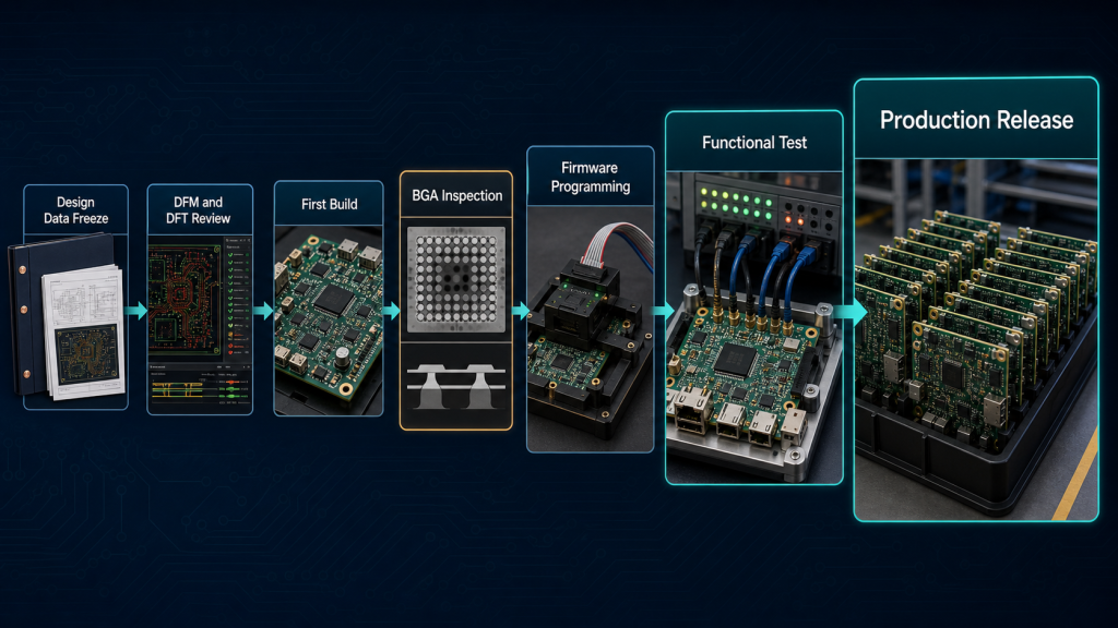
Before production release, iPCB can support a PCB main board through fabrication review, component sourcing, PCBA, BGA inspection, firmware programming and application-specific functional testing. Keeping these activities within one controlled data flow reduces the chance that design, material and test revisions become disconnected. The first production run should be treated as process validation rather than simply as a larger prototype order. Yield, inspection findings, programming results and functional-test failures should be reviewed before the batch size increases. A stable process is achieved when normal production variation no longer depends on engineering intervention. Operators should follow controlled instructions, while measurable limits determine whether each assembly is accepted.
A functional prototype proves that the circuit concept can work. It does not prove that the product can be manufactured repeatedly. The production reliability of a PCB main board is established by consistent design files, verified power behavior, high-speed routing margin, controlled BGA assembly and test coverage linked to the real product functions. Addressing these factors before tooling and material commitments are finalized prevents production problems from becoming expensive redesigns. A PCB main board is ready for volume only when the factory can reproduce its electrical performance without relying on the engineers who built the first prototype.