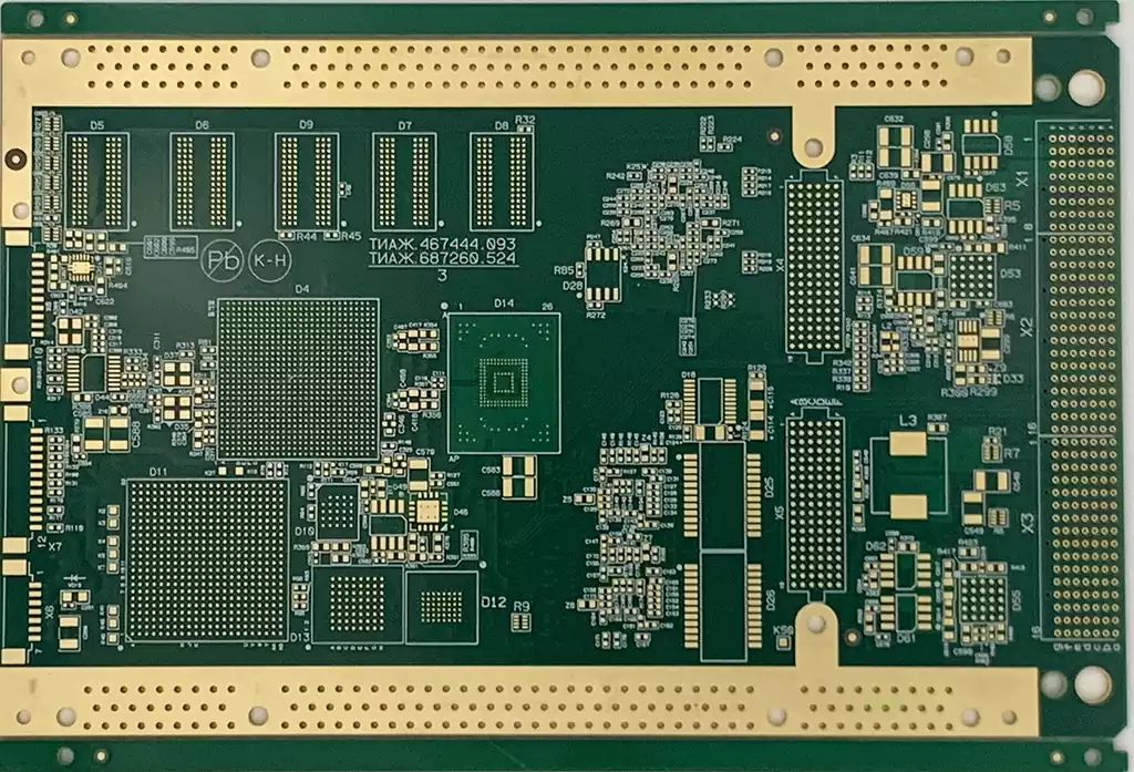
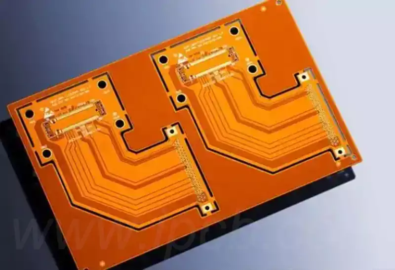
Choosing the best multilayer PCB supplier depends on the requirements of the project rather than on price or production volume alone. A suitable supplier should be able to control the entire manufacturing process, including stack-up design, material selection, lamination, layer registration, via fabrication, impedance control, electrical testing, and final inspection. For high-density or high-speed designs, the supplier’s experience with complex multilayer structures can have a direct impact on signal integrity, manufacturing yield, reliability, and overall project cost.
For this reason, comparing multilayer PCB suppliers requires more than checking a quotation. Engineers and purchasing teams should evaluate whether a manufacturer can consistently produce the required layer count, dielectric structure, copper thickness, trace and spacing, via structure, impedance tolerance, and material system. The supplier should also have sufficient engineering support to identify manufacturing risks before production begins.
What should you look for in a multilayer PCB supplier
A multilayer PCB is more difficult to manufacture than a simple two-layer or four-layer board because the performance and reliability of the finished PCB depend on the interaction between multiple laminated layers. A supplier may be able to manufacture a high-layer-count PCB, but that does not necessarily mean it can maintain the dimensional stability, registration accuracy, dielectric thickness, and electrical characteristics required by a demanding design.
One of the first factors to evaluate is the manufacturer’s multilayer PCB manufacturing capability. Ask about the maximum practical layer count, minimum trace and spacing, minimum finished hole size, copper thickness range, board thickness range, aspect ratio, and registration capability. These specifications should be considered together rather than evaluated individually. A PCB manufacturer may advertise a high maximum layer count, for example, while having more limited capability when fine-line routing, thick copper, tight impedance tolerances, or complex via structures are added to the same design.
The manufacturing process is equally important. Multilayer boards require precise inner-layer imaging and etching before the individual layers are laminated into a single structure. During lamination, temperature, pressure, material characteristics, resin flow, and copper distribution all affect the final board. Poor control at this stage can lead to registration problems, resin starvation, voids, warpage, or changes in finished dielectric thickness.
A capable supplier should therefore be able to discuss the manufacturing risks associated with the actual stack-up instead of simply accepting the supplied Gerber or fabrication files.
Stack-up and lamination are critical to multilayer PCB performance
The stack-up determines much more than the physical order of the copper layers. It affects impedance, signal propagation, power distribution, thermal behavior, mechanical balance, and the manufacturability of the finished PCB.
For high-speed multilayer PCBs, the relationship between signal layers, reference planes, dielectric thickness, and copper thickness needs to be controlled carefully. A supplier with strong engineering capabilities should be able to review the proposed stack-up and identify potential manufacturing or electrical problems before fabrication.
Material selection also needs to be considered as part of the stack-up rather than as an isolated purchasing decision. Standard FR-4 materials are suitable for many applications, but high-speed digital, RF, microwave, high-temperature, and other demanding applications may require materials with different dielectric constant, dissipation factor, thermal characteristics, or dimensional stability.
The supplier should be able to work with the material system specified by the design and maintain consistent processing conditions throughout lamination and subsequent fabrication.
HDI and via capability can determine whether a complex design is manufacturable
As layer counts and component densities increase, conventional through-hole vias may no longer provide enough routing flexibility. HDI structures, microvias, blind vias, buried vias, and sequential lamination can provide additional routing channels and allow designers to reduce board size.
However, these structures also introduce additional manufacturing variables. Microvia formation, via reliability, copper plating, registration between sequential laminations, and dielectric thickness all need to be controlled closely.
When evaluating a multilayer PCB supplier, it is therefore useful to ask not only whether the company manufactures HDI PCBs, but also whether its engineering team understands how HDI structures interact with the proposed stack-up and routing architecture.
For designs with high component density or limited board area, this distinction can be significant. A supplier with experience in both conventional multilayer PCB fabrication and HDI manufacturing is generally better positioned to identify practical alternatives when the original design is difficult to manufacture.
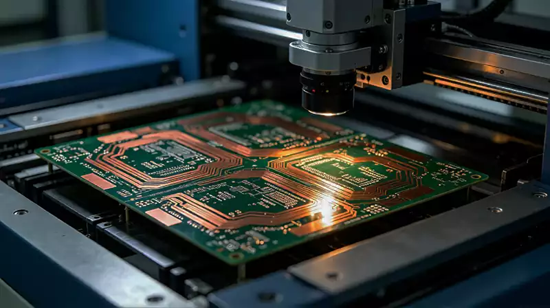
Controlled impedance is important for high-speed multilayer PCBs
Many multilayer PCBs are used in systems where signal integrity is directly affected by PCB geometry and material properties. Interfaces such as high-speed serial links, memory buses, networking systems, RF circuits, and other high-frequency applications may require controlled impedance throughout the signal path.
In these applications, the PCB supplier needs to control parameters such as trace width, copper thickness, dielectric thickness, dielectric constant, and the relationship between signal and reference layers. Manufacturing variation in any of these parameters can affect impedance and insertion loss.
A good supplier should therefore be able to review impedance requirements during engineering rather than treating impedance testing as something that happens only after the board has been fabricated. Test coupons, impedance calculations, cross-section analysis, and appropriate electrical testing can help verify that the finished PCB conforms to the design requirements.
Quality control should be evaluated as part of the manufacturing process
Quality should not be judged only by whether the final boards pass electrical testing. Multilayer PCB reliability depends on process control throughout fabrication.
Inner-layer inspection, AOI, lamination control, drilling, desmear, copper plating, solder mask processing, surface finish, electrical testing, and final inspection all contribute to the quality of the finished board. For complex multilayer designs, cross-section analysis can also provide useful information about plated holes, dielectric thickness, copper thickness, and layer registration.
The appropriate quality requirements depend on the application. A commercial electronics product may have different requirements from an industrial controller, medical device, aerospace system, or high-reliability communication platform. Instead of selecting a supplier based on a generic quality statement, it is better to determine whether the supplier’s inspection and testing process matches the actual reliability requirements of the product.
Engineering support matters before production begins
One of the easiest ways to distinguish PCB suppliers is to look at what happens before the order enters production.
A manufacturer that only processes files and returns a quotation may not identify problems that later cause manufacturing delays. An experienced PCB engineering team can review the design for manufacturability, examine the stack-up, check drill and routing constraints, evaluate copper distribution, and identify areas where the design may create fabrication risks.
This is particularly important for multilayer PCBs because a relatively small change in layer construction can affect several manufacturing parameters at the same time. Early engineering review can reduce the risk of redesign, production delays, and unexpected cost increases.
For this reason, engineering communication should be treated as part of supplier evaluation rather than as an additional service after the purchase order has been placed.
Production capacity is not the same as manufacturing capability
Production volume is another factor, but it should not be evaluated independently from technical capability.
A supplier may be suitable for prototypes but less suitable for stable volume production. Another manufacturer may have strong mass-production capacity but provide limited support for low-volume engineering builds. The right choice depends on the stage of the product and the expected production requirements.
For a new multilayer PCB design, prototype and first-article production may require more engineering interaction and DFM support. Once the design is stable, consistency between production batches becomes increasingly important. The supplier should be able to maintain the specified stack-up, material system, copper thickness, surface finish, and electrical characteristics as production volume increases.
This is why supplier evaluation should consider both the immediate order and the expected lifecycle of the PCB.
How to compare multilayer PCB suppliers
A practical comparison should begin with the technical requirements of the PCB rather than the supplier’s marketing claims. Prepare the main specifications before requesting quotations, including layer count, finished board thickness, copper thickness, minimum trace and spacing, minimum via size, material requirements, surface finish, impedance requirements, HDI structures, expected annual volume, and required certifications or testing.
Then ask each supplier to confirm whether these requirements can be manufactured under normal production conditions.
It is also useful to ask how the supplier handles engineering review. A detailed response that explains potential stack-up, lamination, impedance, drilling, or registration issues is generally more informative than a simple statement that the design is “manufacturable.”
Cost should be considered after these technical requirements have been established. The lowest quotation is not necessarily the lowest-cost solution if it results in additional engineering changes, lower yield, longer lead times, or inconsistent production quality.
For multilayer PCB projects, the better supplier is usually the one that can provide a reliable balance between technical capability, manufacturing consistency, engineering support, quality control, lead time, and total production cost.
Evaluating iPCB as a multilayer PCB supplier
iPCB can be evaluated against the same technical criteria used for any multilayer PCB supplier. The important question is not simply whether a manufacturer can produce multilayer boards, but whether its manufacturing and engineering capabilities match the requirements of the specific project.
For a multilayer PCB project, the evaluation should include the proposed layer structure, materials, lamination construction, copper distribution, via technology, impedance requirements, board thickness, and required inspection and testing. These details provide a much more useful basis for supplier selection than a general statement about PCB manufacturing capability.
When the design involves high-density routing, controlled impedance, complex layer construction, or other demanding requirements, the supplier’s engineering review becomes particularly important. The objective is to confirm that the proposed PCB construction is both electrically appropriate and practical to manufacture at the required quality level.
Before production, customers should also confirm the applicable material specifications, dimensional tolerances, testing requirements, surface finish, production quantity, and quality standards with the manufacturer. These requirements should be defined according to the actual product and application rather than assumed from a general PCB specification.
What information should you provide to a multilayer PCB supplier
A supplier can evaluate a multilayer PCB more accurately when the initial RFQ contains enough technical information. At minimum, the package should normally include the PCB fabrication data, layer count, finished board dimensions, board thickness, copper thickness, material requirements, surface finish, impedance requirements, and required quantity.
For more complex boards, additional information may include the required stack-up, controlled-impedance specifications, HDI or microvia requirements, special material requirements, electrical testing requirements, reliability standards, and any application-specific quality requirements.
Providing this information at the beginning allows the supplier to evaluate manufacturability and provide a quotation based on the actual production requirements.
The best multilayer PCB supplier is not necessarily the manufacturer with the lowest price, the highest advertised layer count, or the fastest standard lead time. The better choice is the supplier whose manufacturing process, engineering capability, quality system, and production capacity are aligned with the requirements of the PCB.
For complex multilayer designs, supplier evaluation should begin with the stack-up and manufacturing requirements and then extend to HDI capability, impedance control, materials, testing, engineering support, production consistency, and total cost. This approach gives engineering and purchasing teams a more reliable basis for selecting a multilayer PCB manufacturing partner.