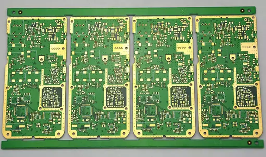
Multilayer PCBs are the core foundation of modern high-end electronic equipment, enabling complex circuit routing, high-density signal transmission, and reliable electrical interconnection. Compared with conventional double-sided PCBs, multilayer PCBs feature a far more sophisticated layer structure, tighter manufacturing tolerances, and more advanced production technologies. Their manufacturing process combines standardized production methods with high-precision engineering.
Today, PCB manufacturers generally do not produce core raw materials such as copper clad laminates (CCLs), prepregs, or copper foil in-house. Instead, these materials are sourced from specialized upstream suppliers and transformed into finished multilayer PCBs through a series of precisely controlled manufacturing processes, including material preparation, circuit pattern formation, lamination, surface protection, and final inspection. This article provides a comprehensive overview of the complete manufacturing process of multilayer PCBs, from raw material preparation to finished product inspection.
Raw Material Cutting and Preparation for Multilayer PCBs
In the production of multilayer PCBs, manufacturers purchase all essential base materials—including copper clad laminates, prepregs, and copper foil—from qualified material suppliers rather than manufacturing these materials themselves. To facilitate transportation and comply with industry-standard supply specifications, these materials are typically delivered in large standardized panel sizes, commonly measuring approximately 1 m × 1 m or 1 m × 1.2 m.
Since these standard panels cannot be processed directly by PCB manufacturing equipment, a panel cutting process must be completed before production begins. Based on the capabilities of the production line and the dimensions required for each multilayer PCB design, manufacturers cut the large panels into standardized production panels suitable for subsequent processes such as inner-layer circuit fabrication and multilayer lamination.
Unlike conventional double-sided PCBs, multilayer PCB manufacturing follows a different process sequence. After the raw material has been cut to size, the inner-layer circuits are fabricated first, followed by multilayer lamination. Only after the multilayer stack has been fully laminated and cured do subsequent processes—including drilling, copper plating, and outer-layer circuit fabrication—follow essentially the same manufacturing flow as that used for double-sided PCBs. After multiple quality inspections and proper packaging, the finished multilayer PCBs are ready for shipment.
Inner-Layer Circuit Fabrication
The inner layers of a multilayer PCB are manufactured using ultra-thin double-sided copper clad laminates, which serve as the conductive foundation for internal signal routing and electrical interconnection between different layers.
The primary objective of inner-layer fabrication is to accurately transfer the designed circuit pattern onto the copper surface. Because the inner-layer circuitry directly determines the electrical performance and signal integrity of the finished PCB, this stage is one of the most critical precision manufacturing processes.
The fabrication process begins by laminating a photosensitive dry film onto the clean copper surface inside a dust-free production environment. A pre-produced phototool containing the inner-layer circuit pattern is then precisely aligned with the panel before exposure equipment transfers the circuit image through ultraviolet light, causing the exposed areas of the dry film to undergo a photochemical reaction.
After exposure, the panel proceeds to the developing process, where the unexposed dry film is removed while the circuit pattern remains protected by the hardened photoresist.
The panel is then processed through an automated chemical etching line, where the exposed copper is selectively removed, leaving only the intended conductive traces. Once etching is complete, the remaining dry film is stripped away, fully exposing the finished inner-layer circuitry.
To ensure high manufacturing quality, every completed inner layer undergoes 100% inspection using an Automated Optical Inspection (AOI) system. AOI accurately detects defects such as open circuits, short circuits, missing copper, line width deviations, and pattern misalignment. Any defective panels are either repaired or rejected before entering the next manufacturing stage.
After passing AOI inspection, each inner-layer panel undergoes a brown oxide treatment, which serves as an essential surface preparation process before lamination and has a direct impact on bonding strength, structural reliability, and long-term product performance.
Purpose of Brown Oxide Treatment
Brown oxide treatment plays several important roles during multilayer PCB manufacturing.
First, it significantly improves interlayer bonding strength by chemically roughening the copper surface, thereby increasing the contact area between the copper foil and the prepreg resin.
Second, it enhances resin wettability, allowing molten resin to flow more effectively into fine circuit gaps and corners during lamination, resulting in a stronger and more uniform laminated structure after curing.
Finally, the process forms a stable passivation layer on the copper surface, preventing undesirable chemical reactions between the copper and curing agents during high-temperature lamination. This effectively reduces the risk of delamination, blistering, and other structural defects.
Multilayer PCB Lamination
After brown oxide treatment, the prepared inner-layer panels are assembled according to the specified layer stack-up defined in the PCB design.
The manufacturing personnel carefully stack the inner-layer circuit boards, prepregs, and outer copper foils in the correct sequence while maintaining precise layer-to-layer alignment and preventing contamination throughout the assembly process.
The completed stack is then transferred to a lamination press, where high temperature and high pressure cause the prepreg resin to melt, flow, and cure. As the resin solidifies, all layers are permanently bonded into a single integrated structure, forming the basic construction of the multilayer PCB.
Lamination is one of the most critical manufacturing processes because it directly determines the structural stability of the finished board. Improper process parameters can easily lead to voids, delamination, warpage, or other defects that significantly affect product quality.
Once lamination is complete and the panel has cooled naturally, the multilayer structure is fully formed, allowing outer-layer processing to begin. From this stage onward, the manufacturing flow generally follows the same procedures used for double-sided PCBs.
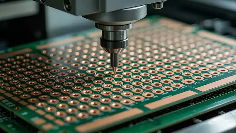
Precision Drilling
Following lamination, each conductive layer inside the multilayer PCB remains electrically isolated. Precision drilling is therefore required to create the vias that establish electrical connections between different layers.
Using high-precision CNC drilling machines, manufacturers drill holes at the exact locations and diameters specified in the PCB design files. These holes provide the foundation for subsequent metallization and interlayer electrical connectivity.
Drilling accuracy has a direct influence on plating quality and long-term electrical reliability, making it one of the most important precision manufacturing operations in multilayer PCB production.
Through-Hole Metallization and Panel Plating
Immediately after drilling, the hole walls consist primarily of insulating resin and therefore cannot conduct electricity. To establish electrical interconnections between layers, manufacturers perform through-hole metallization using chemical copper deposition followed by panel plating.
This manufacturing stage consists of three major processes: desmearing, electroless copper deposition, and full-panel electroplating.
Desmearing
During drilling, friction between the drill bit and the laminate generates heat, causing resin smear to accumulate on the hole walls. At the same time, the hole surface remains relatively smooth, making metal adhesion more difficult.
The desmear process completely removes resin residue while microscopically roughening the insulating hole wall, significantly improving the adhesion between the resin and the subsequent copper deposit and reducing the risk of copper separation or barrel failure.
Electroless Copper Deposition
An electroless copper process uses controlled chemical reactions to deposit a thin and uniform conductive copper layer onto the previously non-conductive hole walls.
This initial copper layer functions as the conductive seed layer required for electroplating and represents a critical step in through-hole metallization.
Full-Panel Electroplating
Using the electroless copper layer as a conductive base, electroplating deposits additional copper across the entire panel, increasing the copper thickness inside the plated through holes until it satisfies both industry standards and product design specifications.
Because the outer circuit pattern has not yet been defined at this stage, the entire panel receives uniform copper plating, which is why this process is commonly referred to as full-panel plating.
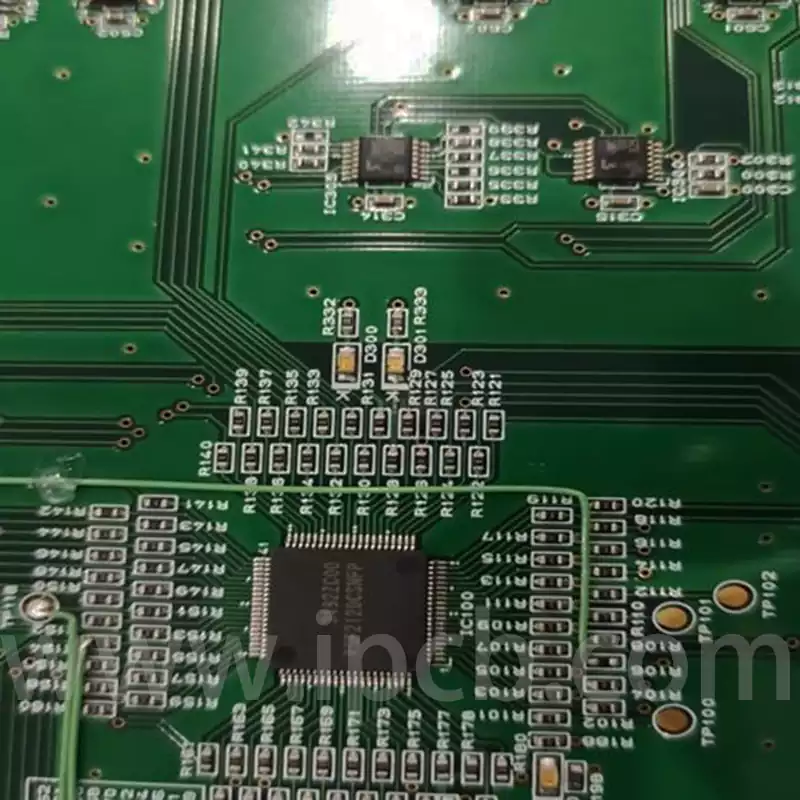
Outer-Layer Circuit Pattern Formation
The objective of this process is to accurately transfer the designed outer-layer circuit pattern onto the external copper surfaces of the multilayer PCB, thereby completing the overall circuit structure together with the previously fabricated inner layers.
The process begins with dry film lamination, followed by image exposure and development, producing a protective resist pattern while exposing only the copper areas that require plating.
Pattern plating is then performed to increase the copper thickness on both the exposed circuit traces and the plated through holes. A layer of tin is subsequently deposited over the plated copper to protect the circuit pattern during the following etching process.
After pattern plating is completed, the dry film is stripped using a sodium hydroxide (NaOH) solution, exposing the unwanted copper outside the protected circuit areas.
Chemical etching then removes all exposed copper, leaving only the required outer-layer circuitry. At this point, both the inner and outer circuits of the multilayer PCB have been fully formed.
Solder Mask Application
Once all circuit patterns have been completed, a solder mask is applied to protect all non-solderable areas of the PCB.
A specially formulated solder mask ink is uniformly coated over the board surface before undergoing exposure, development, and thermal curing to form a durable protective layer that completely covers the non-soldering copper surfaces.
The solder mask protects the copper against oxidation, moisture, contamination, and accidental short circuits. It also prevents solder bridging during component assembly, improves electrical insulation, enhances corrosion resistance, and significantly extends the service life of the finished PCB while clearly defining the soldering areas for automated assembly.
PCB Legend Printing
After the solder mask has fully cured, component markings are printed onto the PCB surface.
Modern PCB manufacturers typically use either screen printing or laser marking to apply reference designators, component identifiers, revision numbers, manufacturer information, and other production markings.
These clear markings facilitate automated assembly, inspection, maintenance, troubleshooting, and after-sales service, making them an essential feature of modern industrial PCB manufacturing.
Surface Finish
The purpose of surface finishing is to protect the exposed copper pads and contact areas that remain uncovered by the solder mask.
Without adequate protection, these exposed copper surfaces rapidly oxidize when exposed to air and moisture, resulting in poor solderability, unreliable electrical contact, and assembly defects.
Depending on the application requirements, manufacturers may apply various industry-standard surface finishes, including Hot Air Solder Leveling (HASL), Electroless Nickel Immersion Gold (ENIG), Immersion Silver, or Organic Solderability Preservative (OSP).
These finishes protect the copper from oxidation while maintaining excellent solderability, electrical conductivity, and long-term reliability.
PCB Profile Routing
After all surface processing has been completed, the PCB panels are machined into their final dimensions according to the customer’s design requirements.
This process removes production rails and excess laminate material, producing the finished PCB outline.
The most common profiling methods include CNC routing, die punching, manual routing, and manual cutting. Among these methods, CNC routing and die punching provide the highest dimensional accuracy and consistency, making them ideal for high-volume, high-precision multilayer PCB production. Manual routing is generally used for small production runs or irregular board shapes, while manual cutting is suitable only for simple, low-precision applications.
Electrical Testing and Final Inspection
After profiling, every multilayer PCB undergoes comprehensive electrical testing using dedicated testing equipment to verify circuit continuity and identify defects that cannot be detected through visual inspection, including open circuits, short circuits, and impedance abnormalities.
Only boards that successfully pass electrical testing proceed to the final visual inspection.
During final inspection, experienced quality inspectors carefully examine every PCB for cosmetic and manufacturing defects. Minor repairable defects are corrected through rework, while nonconforming products are rejected to ensure that only fully qualified multilayer PCBs meeting both customer specifications and industry standards are approved for shipment.