A scanner pcb board can pass basic power and communication tests while the completed machine still produces vertical lines, color variation or random noise. These defects are often blamed on the contact image sensor, optical system or calibration software, but the source may be inside the board’s analog signal path, power distribution or motor-control circuit.
Image quality depends on more than whether every component is correctly soldered. The sensor output must be sampled at the right time, converted without excessive electrical noise and synchronized with document movement. A small disturbance repeated during every scan line can become a highly visible pattern across the final image.
What the Scanner PCB Board Controls
A document scanner normally uses a contact image sensor or CCD to convert reflected light into an analog signal. The scanner control board supplies power to the sensor and light source, generates timing signals, processes the analog output and transfers digital image data to the processor.
The same board may control the paper-feed motor, document sensors and communication interface. This places sensitive image-acquisition circuits close to switching regulators, motor drivers and fast digital signals.
The scanner pcb board must therefore support two different electrical environments. The sensor and analog front end require stable references and low-noise power, while the motor and digital circuits produce rapidly changing current. Visible defects appear when these circuit domains interfere with one another.
Fixed Lines Usually Follow One Signal Channel
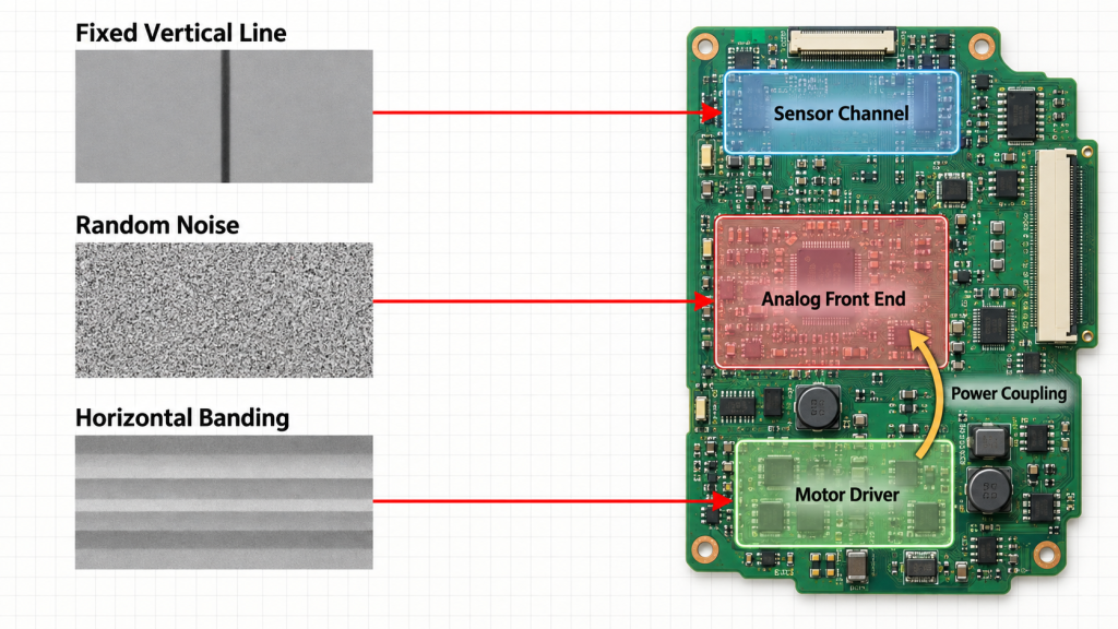
A vertical line that remains in the same image position normally points to a repeatable error in the sensor signal chain. One sensing element may have a different dark level, one analog channel may contain an offset or one connection may be unstable.
The sensor produces a sequence of pixel values for every scanned line. If the same pixel or channel consistently reports an incorrect value, the error is repeated at the same horizontal position. Once the lines are assembled into a complete image, that repeated error becomes a vertical stripe.
Analog Devices describes contact image sensor outputs as line-based analog waveforms that must be sampled before digitization. The timing relationship between the sensor clock, line-start pulse and sampling circuit affects the captured pixel value. Analog Devices sensor signal processing guide
Several board-level faults can cause this pattern. A marginal sensor connector may interrupt one channel. Excessive resistance in a reference or ground connection can shift the analog level. Contamination near a high-impedance input may create leakage that changes with humidity or temperature.
When a scanner pcb board produces a fixed vertical line, replacing the sensor without checking its electrical channel may only provide a temporary result. The image position should be compared with the corresponding sensor output, connector contact and analog-front-end input.
Random Noise Enters Through the Analog Path
Random speckles or grain indicate a different problem. The pattern changes between scans because the disturbance is not tied to one sensor element.
Sensor output can be relatively small in dark or low-reflectance areas. Noise entering before analog-to-digital conversion may then become more visible after gain and image processing are applied. A white document may appear acceptable while photographs and gray areas reveal strong noise.
The complete analog path includes the sensor output, amplifier, ADC input, voltage reference, power supply and return path. Any of these points can allow interference to enter the image.
A switching regulator placed too close to the analog front end can couple noise through copper planes or magnetic fields. Fast clock traces may inject current into a shared return path. A long sensor connection can receive interference from memory, communication interfaces or motor cables.
Grounding must control where these currents return. Splitting ground without considering signal flow can force analog current through a long path. Connecting every ground region without controlling motor current can allow switching noise to pass through the same copper used by the sensor reference.
Analog Devices notes that low-noise sensor readout requires a precision analog front end and careful PCB layout to prevent high-power switching signals from coupling into sensitive circuits. Analog Devices image sensor reference design
This is why scanner image noise cannot always be corrected by adding one capacitor. The disturbance source, coupling path and affected signal must be identified together.
Motor Interference Creates Horizontal Bands
The paper-feed motor draws current in pulses as the driver switches its windings. If this current changes the sensor supply or ground reference, the disturbance may appear as horizontal bands across the scanned page.
Band spacing provides a useful diagnostic clue. A pattern that changes with scan speed, motor stepping rate or mechanical load is more likely to come from the motion-control section than from a fixed sensor defect.
A multimeter may show an acceptable supply voltage because it averages rapid changes. An oscilloscope measurement taken close to the sensor or analog front-end supply is more useful. The motor should be operating under realistic load during this measurement.
On a scanner pcb board, motor current should return to its source without passing through the sensor reference region. Driver decoupling should remain close to the switching stage, and high-current loops should be compact. Sensor and motor cables should not run together if their proximity creates magnetic or capacitive coupling.
Not every horizontal band is electrical. An irregular feed rate changes the distance represented by each captured line. This mechanical error can resemble power interference. Comparing the image pattern with the motor-control timing helps separate electrical noise from inconsistent document movement.
Illumination Power Affects Brightness and Color
Some contact image sensor modules integrate the LED source, lens and sensor. ON Semiconductor documentation shows a typical scanner architecture containing the CIS module, conversion electronics, timing control and motor-control stage. onsemi contact image sensor data sheet
If LED current changes during scanning, image brightness changes with it. In a color scanner, unstable red, green or blue illumination can produce color bands rather than simple dark lines.
The scanner pcb board must prevent illumination pulses from disturbing the analog reference. Local decoupling, controlled current paths and stable LED-driver components are important because the light source and sensor may share part of the same power network.
An incorrect current-setting resistor or weak LED-driver joint can affect an entire color channel. This defect may appear optical even though its origin is electrical.
Assembly Defects May Be Intermittent
A partially soldered sensor connector or cracked passive component may remain conductive during initial testing. As the assembly warms, material expansion can change the connection and alter image quality.
Fine-pitch sensor connectors deserve particular attention because power, clock and analog signals often occupy adjacent contacts. Insufficient solder may create an intermittent channel, while bridging can allow one signal to disturb another.
AOI can identify visible placement and soldering problems, but it cannot prove that the complete acquisition path produces a clean image. Inspection should therefore be combined with functional scanning.
Calibration Cannot Stabilize Hardware
Scanner calibration compensates for predictable differences between sensor elements, LED brightness and analog channels. It is useful when these differences remain stable.
Calibration cannot permanently correct a signal that changes with motor current, temperature or connector movement. The image may look correct immediately after calibration and develop lines later during operation.
Increasing software correction can conceal a manufacturing problem while reducing useful image range. The scanner pcb board should first produce a stable raw signal. Calibration should correct repeatable channel variation rather than compensate for unstable electronics.
Testing Must Include Real Images
Power, firmware and communication tests do not verify scan quality. The finished assembly must capture a controlled target while the sensor, LEDs and paper-feed motor operate together.
A suitable target can reveal fixed lines, brightness variation, color-channel differences, missing pixels and geometric distortion. Gray and dark areas are especially useful because they expose noise that may disappear on white paper.
More than one scan should be evaluated. A marginal scanner pcb board may pass immediately after startup and fail after its temperature or motor load changes.
In production, image-analysis software can measure uniformity, noise and alignment against defined limits. The acceptance result should be linked to the hardware revision, firmware version and board batch.
For scanner products moving into production, iPCB can combine PCB fabrication, sensor-interface assembly, connector inspection, programming and image-based functional testing within one controlled manufacturing flow. This makes it easier to trace an image defect back to the relevant component or process record.
Clean Images Require Stable Electronics
A scanner pcb board influences every stage between sensor exposure and the final digital image. Fixed vertical lines may follow an individual channel, random noise can enter through the analog path, and horizontal bands may reflect interaction between the sensor and motor-control circuits.
Diagnosis should begin with the pattern visible in the image and work backward toward its electrical or mechanical source. Replacing the sensor or changing calibration without identifying the coupling path may only hide the defect.
When sensor timing, power, grounding, illumination and movement are validated together, a scanner pcb board can maintain consistent image quality across different scan speeds, operating temperatures and production batches.