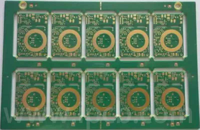
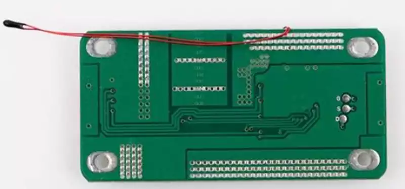
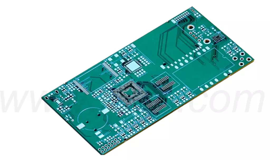
Multilayer PCB fabrication is the process of manufacturing a printed circuit board with three or more conductive copper layers separated by insulating dielectric materials. Unlike a single-sided or double-sided PCB, a multilayer board contains several internal circuit layers that are aligned, laminated, drilled, plated, and electrically connected to form one finished board.
Multilayer PCBs are widely used when a circuit requires more routing space, better power distribution, controlled impedance, or a higher component density than a two-layer board can provide. A typical multilayer PCB may contain four, six, eight, or more copper layers, with each layer assigned to signal routing, power distribution, grounding, or other specific functions.
The fabrication process becomes more demanding as the number of layers increases. Layer-to-layer registration, lamination, drilling, copper plating, material selection, and electrical testing all have to be carefully controlled because an error inside the stack-up may not be visible from the finished board surface.
What Is Multilayer PCB Fabrication?
Multilayer PCB fabrication combines several patterned copper layers with insulating dielectric layers to create a single rigid circuit structure.
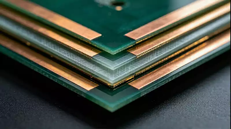
A typical multilayer stack-up consists of copper layers, laminate cores, and prepreg materials. The copper layers carry electrical signals or distribute power and ground, while the dielectric materials electrically isolate adjacent copper layers and provide mechanical support.
For example, a four-layer PCB may use the outer layers primarily for component connections and signal routing, while one or more internal layers are dedicated to power and ground. More complex boards can use additional signal layers to provide enough routing space for high-density circuits.
The main advantage is that the circuit no longer has to fit entirely on the top and bottom surfaces. Internal copper layers provide additional routing channels without requiring a proportional increase in board size.
This makes multilayer construction particularly useful when a product needs to combine a compact form factor with a relatively complex electrical design.
Why Does Multilayer PCB Fabrication Require More Process Control?
The main difficulty with multilayer fabrication is that the manufacturer is not simply producing several individual copper layers. Those layers must eventually become one accurately aligned structure.
A small registration error during lamination can affect the position of pads and vias relative to the internal circuitry. Drilling also becomes more demanding because a hole may need to connect several internal layers at precisely defined locations.
The fabrication process therefore depends on controlling several variables at the same time. Material movement, copper distribution, lamination conditions, drill accuracy, hole-wall quality, plating thickness, and layer registration can all influence the finished board.
This is why multilayer PCB fabrication normally begins with an engineering review before the manufacturing process starts. The manufacturer needs to determine whether the proposed layer stack-up, trace geometry, drill structure, material system, finished thickness, and other requirements are compatible with the production process.
The Multilayer PCB Fabrication Process
Although the exact workflow varies according to the board construction and manufacturing technology, a conventional multilayer PCB generally passes through several major stages.
Engineering Review and CAM Preparation
The manufacturing process begins with the customer’s design data. Gerber or ODB++ files, drill data, board dimensions, layer information, material requirements, surface finish, impedance requirements, and fabrication notes are reviewed before production.
The engineering team checks important manufacturing parameters such as trace width, spacing, annular ring, drill sizes, copper thickness, and clearances. The stack-up is also reviewed to make sure the proposed construction can be manufactured consistently.
At this stage, manufacturing data may be adjusted to compensate for expected dimensional changes during processes such as etching and lamination.
This front-end engineering stage is particularly important for multilayer boards because a problem discovered after lamination can be much more difficult and expensive to correct.
Inner Layer Imaging and Etching
The inner copper layers are manufactured before the complete board is laminated.
A photoresist is applied to the copper surface, and the circuit pattern is transferred to the board using imaging equipment. After development, the exposed copper is etched away, leaving the required circuit pattern.
The finished inner layers are then inspected to confirm that the traces and clearances correspond to the design data.
Automated optical inspection, commonly known as AOI, is widely used to identify defects such as unwanted copper, missing features, opens, shorts, and pattern deviations before the layers are assembled. Inner-layer inspection is important because these circuits will become inaccessible after lamination.
Inner Layer Preparation
After imaging and inspection, the inner layers undergo surface preparation before lamination.
The copper surfaces need to provide reliable adhesion to the dielectric material during the pressing process. Surface treatments such as oxide or alternative bonding treatments may be used depending on the manufacturing process and material system.
The objective is to create a stable interface between the copper and dielectric layers while maintaining the dimensional characteristics required by the stack-up.
Stack-Up and Lamination
Lamination is one of the most important stages in multilayer PCB fabrication.
The individual copper layers, laminate cores, and prepreg materials are arranged according to the approved stack-up. The complete assembly is then subjected to controlled heat and pressure so that the dielectric material bonds the layers into a single structure.
The stack-up determines much more than the final board thickness. It influences signal integrity, impedance, power distribution, thermal behavior, mechanical stability, and the manufacturability of the finished PCB.
During lamination, the materials can experience dimensional movement. The amount of movement depends on factors such as material properties, copper distribution, layer position, and the lamination process. Consequently, manufacturers need to account for these changes when preparing fabrication data.
Poor lamination control can result in problems such as delamination, voids, thickness variation, or registration errors. For high-layer-count boards, maintaining accurate alignment throughout the stack becomes increasingly important.
Drilling
Once the multilayer stack has been laminated, holes are drilled according to the design requirements.
Through-holes can pass through the entire board and provide electrical connections between multiple layers. Depending on the board construction, blind or buried vias may also be used, although these technologies can require additional manufacturing processes.
Mechanical drilling is commonly used for conventional through-holes. More advanced multilayer and HDI constructions may use laser drilling for smaller interconnections and microvias.
The drilling process must account for factors such as hole diameter, board thickness, aspect ratio, positional accuracy, and the materials used in the stack-up.
Desmear and Copper Plating
After drilling, the hole walls consist largely of non-conductive laminate material and cannot yet provide an electrical connection between copper layers.
The hole walls therefore undergo cleaning and preparation processes before copper is deposited. A thin electroless copper layer is typically deposited to create a conductive surface, followed by electrolytic copper plating to build the required copper thickness.
This process creates the plated-through-hole structure that electrically connects the appropriate copper layers.
Hole-wall quality is particularly important for multilayer PCBs because the plated barrel may be exposed to mechanical and thermal stresses during assembly and operation. The fabrication process therefore needs to provide consistent adhesion and copper coverage throughout the hole.
Outer Layer Imaging and Etching
After the internal connections have been established, the outer copper layers are patterned.
Photoimaging and etching are used to create the traces, pads, and other copper features on the top and bottom surfaces. The outer-layer pattern must align correctly with the internal structure and drilled features.
For dense designs, the relationship between the outer-layer pads and internal vias becomes increasingly important. Registration errors can reduce annular ring dimensions or create clearance problems, which is why dimensional control is a major consideration in multilayer PCB fabrication.
Solder Mask and Surface Finish
After the circuit pattern has been completed, a solder mask is applied to protect most of the exposed copper while leaving pads and other required areas accessible for soldering.
A surface finish is then applied to exposed copper areas to protect them from oxidation and provide suitable solderability. The appropriate finish depends on the application, assembly process, reliability requirements, and design specifications.
Common surface finishes include ENIG, OSP, immersion tin, and other plating systems. The choice should be considered together with component requirements, soldering conditions, storage requirements, and the intended service environment.
Electrical Testing and Final Inspection
The final manufacturing stages include board profiling, visual inspection, dimensional checks, and electrical testing.
Electrical testing verifies that the fabricated circuit has the required continuity and isolation characteristics. Depending on the product and customer requirements, additional inspections may be performed to verify board thickness, copper features, hole quality, surface finish, solder mask, and other characteristics.
Testing is especially important for multilayer boards because internal defects may not be visible during a normal visual inspection.
Materials Used in Multilayer PCB Fabrication
Material selection has a direct influence on the performance and manufacturability of a multilayer PCB.
Conventional multilayer boards commonly use glass-reinforced epoxy laminate systems, with copper foil forming the conductive layers. Prepreg is used between certain copper layers as an insulating and bonding material, while core materials provide a stable dielectric structure.
The material system needs to match the electrical, thermal, mechanical, and manufacturing requirements of the design.
For high-speed applications, dielectric properties and layer-to-layer spacing become particularly important because the stack-up can affect controlled impedance and signal propagation. For applications exposed to elevated temperatures or demanding thermal cycling, material characteristics such as glass transition temperature and coefficient of thermal expansion may also become important design considerations.
The material should therefore be selected as part of the overall stack-up rather than treated as an isolated purchasing decision.
What Makes High-Layer-Count PCB Fabrication More Difficult?
Increasing the layer count does not simply add more copper to the same manufacturing process. It introduces additional opportunities for dimensional variation and registration errors.
As more layers are added, the manufacturer has to maintain accurate relationships between a larger number of internal features. The board also becomes more sensitive to the effects of lamination, drilling, copper distribution, and thermal expansion.
High-layer-count designs can also require more sophisticated stack-up planning. Signal layers may need to be positioned relative to reference planes to support impedance control and reduce unwanted coupling. Power and ground layers may be arranged to provide an appropriate distribution network.
For very dense designs, conventional through-hole technology may not provide enough routing flexibility. HDI construction, blind vias, buried vias, microvias, and sequential lamination can then be considered. HDI fabrication introduces additional process cycles and tighter manufacturing controls compared with conventional multilayer PCB production.
DFM Considerations for Multilayer PCB Fabrication
A multilayer PCB should be designed with fabrication limitations in mind rather than treated as a purely electrical design problem.
Trace width and spacing need to match the manufacturer’s capabilities. Drill sizes should be selected with the board thickness and aspect ratio in mind. Via structures should also be reviewed carefully, particularly when blind, buried, or microvias are involved.
The stack-up deserves special attention because it affects finished thickness, impedance, copper distribution, lamination, and mechanical stability.
Designers should also avoid unnecessary complexity. Adding layers, unusual materials, extremely small features, or specialized via structures can increase manufacturing difficulty without necessarily improving the final product.
A good DFM review therefore asks a simple question: can the intended electrical performance be achieved with a structure that can also be manufactured consistently?
How to Choose a Multilayer PCB Fabrication Process
The appropriate fabrication process depends on the actual requirements of the circuit rather than simply the number of layers.
A straightforward four-layer PCB may only require conventional multilayer fabrication with through-holes. A high-speed communication board may require controlled impedance, carefully designed reference planes, and tighter control of dielectric thickness. A compact product with fine-pitch components may require HDI technology and sequential buildup.
Before production, the manufacturing requirements should therefore be defined clearly. Important information includes the layer count, stack-up, finished board thickness, copper thickness, material type, minimum trace and spacing, via structure, impedance requirements, surface finish, and applicable testing requirements.
Providing complete manufacturing information early in the project allows the fabrication process to be reviewed before production and reduces the likelihood of design changes later.
Multilayer PCB fabrication is a coordinated manufacturing process in which electrical design, materials, mechanical construction, and process control all have to work together. The basic workflow may appear straightforward—fabricate the inner layers, laminate the stack, drill and plate the board, form the outer layers, apply the final finishes, and test the finished PCB—but each stage can affect the reliability of the next one.
The most important consideration is therefore not simply how many layers a PCB contains. The stack-up, materials, interconnections, manufacturing tolerances, and electrical requirements all need to be considered as one system.
When these factors are addressed during the design and engineering stages, multilayer PCB fabrication becomes more predictable, and the finished board is more likely to meet its intended electrical and mechanical requirements.