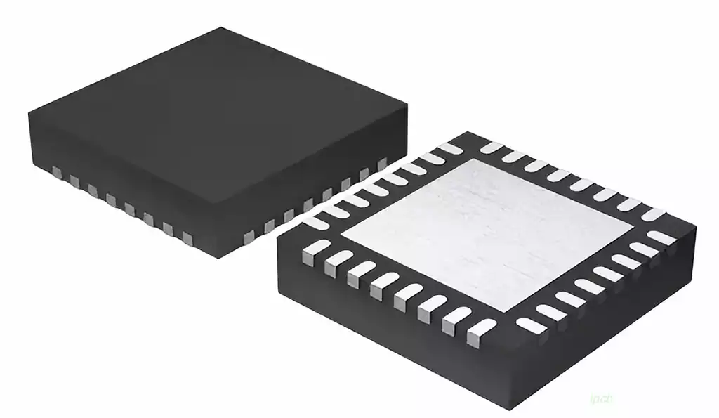
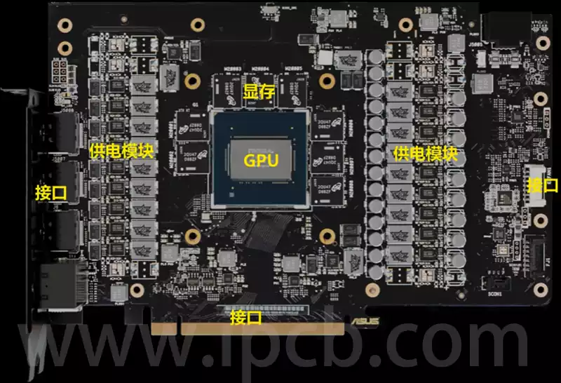
In the vast sea of modern electronics, if chips are the “brain” driving the Internet of Things, then printed circuit boards (PCBs) are the “skeleton and meridians” supporting the operation of these brains and transmitting nerve signals. With the rapid evolution of technology, cutting-edge fields such as 5G communication, artificial intelligence, aerospace, and autonomous driving place almost stringent demands on the size, performance, and reliability of electronic devices. Traditional single-sided or double-sided boards can no longer accommodate such dense components and complex signal transmission requirements, leading to the development of multilayer PCBs.
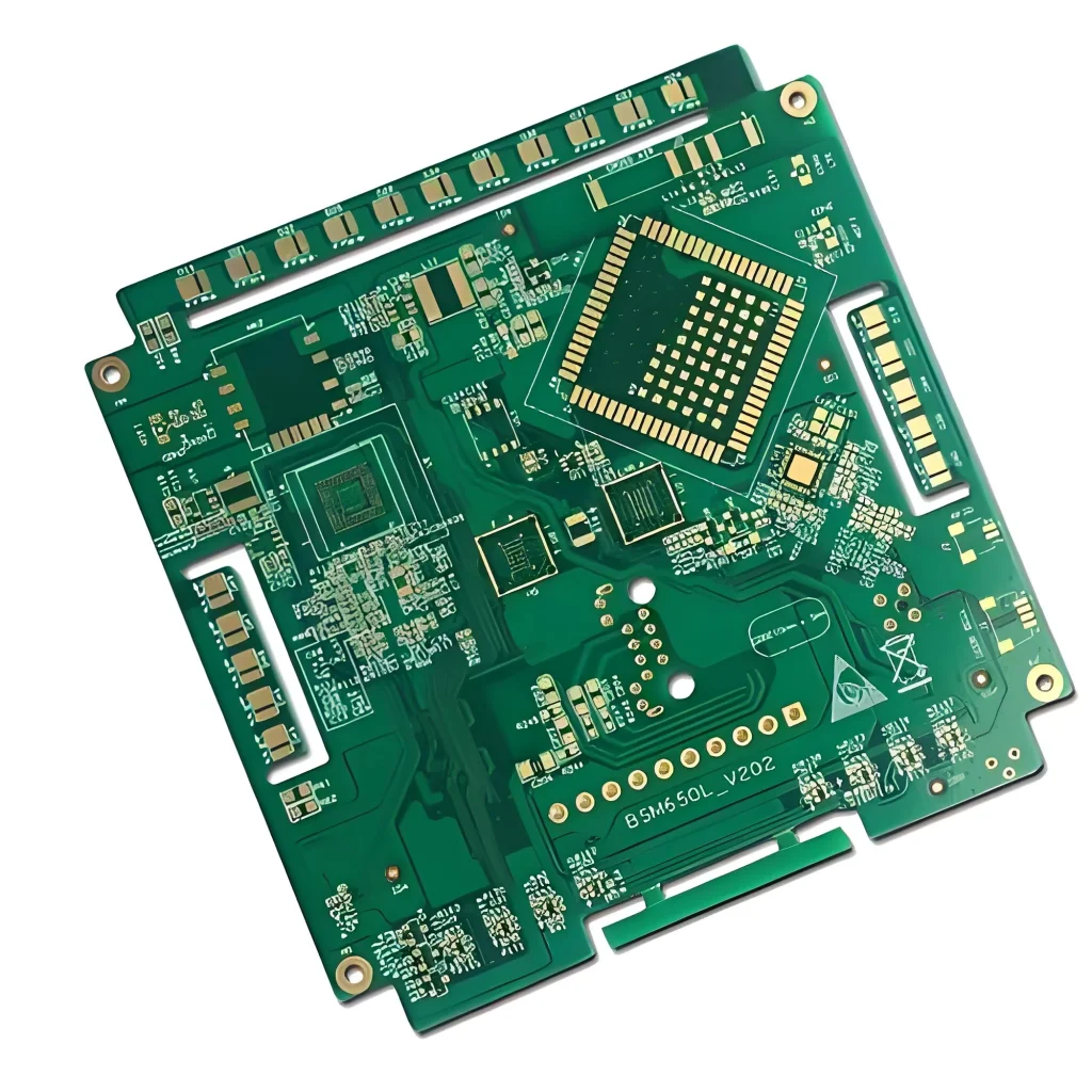
Before multilayer boards can truly achieve mass production, there is a crucial and indispensable step: multilayer PCB prototyping. This is not merely a simple trial production process; it represents the first major leap from abstract engineering design drawings to a concrete physical entity, a “touchstone” for verifying design logic, identifying potential risks, and validating material performance. Today, we will peel back the layers to explore the intricate processes and profound engineering wisdom behind multilayer PCB prototyping.
From Plane to Three-Dimensional Architecture
To understand the complexity of multilayer PCB prototyping, we must first understand the essence of multilayer architecture. Traditional double-sided boards only have a top and bottom layer for routing. As circuit complexity increases exponentially, the limited two-dimensional planar space is quickly filled with traces, making routing impossible. More critically, in high-speed signal transmission, if the signal lines are too far from or discontinuous with the reference ground plane, it can cause severe electromagnetic interference (EMI), signal crosstalk, and impedance mismatch.
Multilayer boards, by alternately stacking multiple conductive pattern layers with insulating dielectric layers, elevate two-dimensional planar routing to a three-dimensional space. In a typical multilayer architecture, engineers not only have more signal layers to manage the intricate interconnections, but more importantly, they can introduce complete power and ground layers. These large copper foil planes not only provide an extremely stable power supply to the system but also act as a robust shield, enveloping sensitive high-frequency signals and greatly improving signal integrity.
The primary task in the prototyping stage is to verify the rationality of this complex three-dimensional stacking design. Because in EDA (Electronic Design Automation) software, everything is a perfect ideal state, but the real physical world is full of variables. Prototyping transforms design drawings into physical prototypes, allowing engineers to test circuit performance in real electromagnetic and thermal environments—something no computer simulation can fully replace.
Material Selection and the Interplay of Physics and Chemistry
The first step in multilayer PCB prototyping isn’t the roar of machines, but the careful selection of materials. Materials determine the PCB’s DNA.
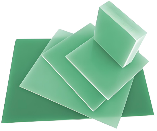
In multilayer boards, the most basic materials are copper-clad laminate (Core) and prepreg. For typical consumer electronics prototypes, standard epoxy fiberglass cloth (such as traditional FR-4) is often sufficient. However, when prototyping involves high-frequency radio frequency, microwave communication, or extremely high-speed digital signals, the dielectric constant and loss tangent of the materials become crucial to success.
At this point, prototyping engineers must introduce more advanced substrates. For example, Rogers’ high-frequency materials, renowned in the industry, or high-performance copper-clad laminates from well-known brands like Shengyi. These materials utilize special resin systems (such as PTFE or hydrocarbon resins) to maintain extremely low energy loss in high-frequency alternating electric fields, ensuring signal purity and stability during transmission. These materials are selected during the prototyping stage to accurately test their true impedance performance at specific operating frequencies.
Besides the substrate, the choice of copper foil also holds significant implications. In high-speed signal prototyping, the current exhibits a “skin effect,” meaning that high-frequency current tends to flow on the surface of the copper foil. If traditional electrolytic copper foil is used, its rough microscopic surface (like undulating mountains) will lengthen the signal transmission path and increase conductor loss. Therefore, high-end multilayer board prototyping often specifies the use of reverse copper foil (RTF) or even extremely low profile copper foil (HVLP) to ensure smoothness at the microscopic level. These subtle considerations at the material level reflect the depth of multilayer board prototyping.
Microscopic engraving and rigorous testing of the inner layers
Once all materials are ready, prototyping officially enters the substantive manufacturing stage. Multilayer board fabrication grows from the inside out; the first step is to process the inner core board.
The formation of the inner layer circuitry is essentially a microscopic magic of light, shadow, and chemistry. First, a layer of UV-sensitive dry-film photoresist is applied to the clean, flawless surface of the inner layer copper foil. Then, a film negative printed with the inner layer circuitry pattern is placed on top and exposed to strong UV light. Light passes through the transparent areas of the film, causing the dry film to polymerize and harden; the black areas block the light, leaving the dry film intact.
After being treated with a developer, the unexposed dry film dissolves, revealing the underlying copper that needs to be removed. Next, a powerful chemical etching solution washes over the exposed copper, leaving only the intricate, labyrinthine inner layer circuitry protected by the hardened dry film. Finally, the protective film is removed, and the physical structure of the inner layer begins to take shape.
But this is only the beginning. During the prototyping stage, even a tiny short circuit (residual copper shavings) or open circuit (broken circuitry) can render the entire prototype unusable. Therefore, the inner layer boards must undergo rigorous inspection by automated optical inspection (AOI) equipment. High-resolution cameras scan the entire board surface at extremely high speeds, comparing it pixel-by-pixel with the original CAM design data. Only flawless inner layer boards qualify for the next crucial stage.
The Art of Lamination and the Symphony of Thermodynamics
The core secret of a multilayer board lies in lamination. This is the process of fusing the dispersed inner core boards and prepreg into a single, indestructible, three-dimensional multilayer structure.
Before lamination, to increase the adhesion between the smooth copper surface and the resin, and to prevent delamination due to heat during use, the inner layer circuitry must undergo browning or blackening treatment. This is a surface oxidation process that generates a layer of microscopic, fluffy copper oxide crystals on the copper surface, greatly increasing the surface area, like countless tiny tentacles ready to firmly grasp the melting resin.
Following this is the precise stacking process. In a cleanroom, operators alternately stack the inner core boards and prepregs according to a pre-designed stackup structure. The prepreg is currently in its B-stage state, meaning the resin is partially cured but still retains fluidity.
The stacked boards are then fed into a vacuum press. Here, a symphony of thermodynamics begins. Under vacuum (to remove interlayer air and prevent bubble formation), the press heats and pressurizes according to strictly defined temperature and pressure profiles. The resin in the prepreg remelts at high temperatures, flowing like magma, filling every gap between the inner layer circuits, even encapsulating every browned copper strand. As the temperature continues to rise, the resin undergoes a cross-linking reaction, transforming from a liquid to a rock-solid C-stage solid.
In multilayer board prototyping, lamination is a challenging process fraught with variables. Engineers need to closely monitor the resin flow and the uniformity of the dielectric thickness after lamination. Even slight deviations in dielectric thickness can cause the final signal line impedance to deviate from the design value. For hybrid laminates (such as prototyping designs that combine high-frequency materials with ordinary FR4 material to save costs), the different coefficients of thermal expansion (CTE) of the materials make the determination of lamination parameters crucial in the prototyping stage. Even slight errors can lead to board warping and deformation.
Breakthroughs in penetrating multilayer drilling and micro-vias:
Although the circuitry layers of a multilayer board are separated by insulating materials, electrical connections must be established at specific locations, which relies on drilling technology.
Traditional mechanical drilling uses micro tungsten carbide drill bits at ultra-high speeds of tens or even hundreds of thousands of revolutions per minute to precisely drill through-holes into the board. During the prototyping stage, engineers rigorously inspect the hole wall roughness and for any nail-head defects, as these directly affect the quality of subsequent hole metallization.
However, with the widespread adoption of High-Density Interconnect (HDI) technology, modern multilayer board prototyping often requires handling extremely small blind and buried vias. Traditional mechanical drills are inadequate for micro-holes smaller than 0.15 mm in diameter and are prone to breakage. This is where laser drilling technology comes in.
A laser beam carries enormous energy, instantly vaporizing resin and glass fiber. Precise control of the laser via hole diameters is a core technology in prototyping. Excessive energy can damage the underlying inner layer target pads; insufficient energy can lead to electrical connection failure due to residual resin at the bottom of the hole.
In this process, the design and manufacturing alignment accuracy of the core capture pads on the inner core board that receive the laser holes is particularly critical. During multilayer lamination, slight misalignment (expansion/contraction) between layers is inevitable. Poor alignment control during prototyping can cause the laser-drilled hole to deviate from the capture pads, resulting in open circuits or reliability issues. Therefore, prototyping is not only about verifying the circuit but also about pushing the factory’s process capabilities to their limits.
Hole Wall Metallization and Outer Layer Shaping
After drilling, the multilayer board still contains insulating resin and fiberglass inside the holes, and the layers are not yet connected. The subsequent electroless copper plating and electroplating processes will give these holes a life-giving electrical current.
Because the hole walls are insulating, a very thin layer of chemical copper must first be deposited on the hole walls as a conductive seed layer through a chemical reaction. Subsequently, through electroplating, driven by current, copper ions continuously crystallize and deposit on the hole walls and surface until a thick and dense copper layer is formed on the inner wall of the hole, firmly connecting all the circuit layers together. In multilayer board prototyping, ensuring that the copper layer thickness at the center of deep holes (holes with high aspect ratios) meets the standard is a key indicator for evaluating the plating uniformity of the electroplating solution.
After hole metallization, the outer layer circuitry is fabricated. Its process principle is similar to the inner layers, involving lamination, exposure, development, and etching. The difference lies in the outer layer, which typically employs patterned electroplating. A layer of etch-resistant metal (usually tin) is plated onto the traces and holes that need to be preserved. Then, the unwanted base copper is etched away, and finally, the tin protective layer is removed, exposing the clean outer copper traces.
With this protective layer and meticulous surface treatment,
the multilayer board now possesses complete electrical functionality. However, exposed copper is highly susceptible to oxidation in air and can easily cause short circuits during subsequent component soldering. Therefore, it needs a robust protective layer—the solder mask, usually the green solder mask we see. Of course, black, blue, or red solder mask can be customized according to customer requirements during prototyping.
The solder mask not only provides moisture protection and insulation but also prevents solder from spreading in non-soldering areas during wave soldering or reflow soldering. Above the solder mask, white character markings (silkscreen) are printed using silkscreen or inkjet printing technology to indicate the location, polarity, and version number of components, providing guidance for subsequent assembly.
Finally, the exposed solder pads must undergo surface finishing. A variety of surface finishing processes are commonly used in multilayer PCB prototyping. For example, OSP (Optically Oriented Film Preservative) forms an organic protective film on the copper surface, offering low cost and good flatness; while ENIG (Enhanced Electroless Gold) chemically deposits a layer of nickel and a layer of gold on the copper surface. Gold’s strong inertness provides long-term protection against oxidation of the pads, and the surface is extremely smooth, making it ideal for fine-pitch BGA chip mounting. The choice of surface finishing during the prototyping stage depends on the prototype’s subsequent storage time, soldering process, and cost considerations.
Final Judgment and Electrical Verification
When a multilayer PCB prototype has completed all physical and chemical tests and is presented to engineers, it cannot be directly sent to the customer. It must undergo final “judgment”—rigorous electrical testing.
Unlike the bed-of-needle testing commonly used in mass production (which is costly and time-consuming to manufacture fixtures), multilayer PCB prototyping typically uses flying probe testing. Several highly flexible probes move at high speed across the board surface, testing each netlet for open circuits and short circuits between adjacent netlets according to the netlist in the design data. While flying probe testing is time-consuming per chip, it eliminates the need for custom fixtures, perfectly suited to the rapid iteration and variable design characteristics of the prototyping stage.
Besides basic continuity testing, impedance testing is an indispensable step for multilayer boards involving high-speed signals. Using a time-domain reflectometer (TDR), a step signal is sent to the test coupon. By analyzing the reflected electromagnetic waves, the actual characteristic impedance of the signal line is accurately calculated. Only when the actual impedance closely matches the design target (typically within ±10%) is the multilayer board prototype considered truly合格 (qualified), proving that its lamination structure, material dielectric properties, and line etching precision meet the requirements for high-speed transmission.
Epilogue: Prototyping – A Bridge Between Ideals and Reality
In summary, multilayer PCB prototyping is far more than simple “small-batch replication”; it is a systematic engineering project integrating materials science, polymer chemistry, precision optics, thermodynamics, and microelectronics. From the initial selection of high-frequency substrates to the light and shadow engraving of inner layer circuits; from resin rheology under high temperature and pressure to the precise ablation of micron-level laser blind vias; every step is filled with challenges to physical limits and the ultimate pursuit of process details.
The core value of prototyping lies in “trial and error” and “verification.” It allows engineers to discover potential problems in the design, optimize manufacturing processes, and verify the limits of materials at extremely low cost before investing millions in large-scale mass production. In this era of rapid technological iteration, high-quality, high-efficiency multilayer board prototyping not only shortens the development cycle of new products but also serves as a powerful driving force for the entire electronics industry to continuously evolve towards lighter, thinner, faster, and more reliable products. Every successfully lit prototype board silently proclaims the birth of a new technology; they are solid bridges connecting engineers’ grand visions with the future intelligent life of humanity.