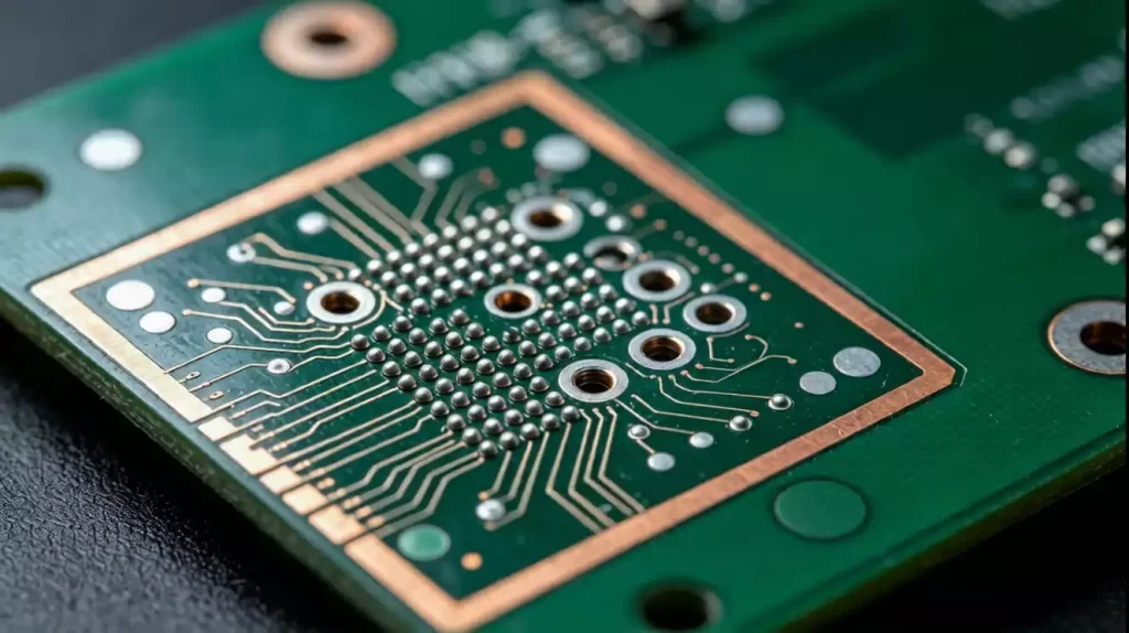
High density circuit boards are designed to accommodate more electrical connections and components within a limited board area. As electronic products continue to become smaller while integrating more functions, conventional PCB structures eventually reach their routing limits. Fine-pitch components, high-pin-count packages, high-speed interfaces, and increasingly compact product enclosures all place greater demands on the available routing space. High density PCB technology addresses these limitations through finer traces and smaller trace spacing, microvias, carefully planned layer structures, and advanced interconnection technologies.
High density does not simply mean increasing the number of PCB layers. The actual routing density depends on how efficiently components, traces, vias, and interconnection structures are arranged within a limited area. A well-designed high density circuit board can use advanced via structures to create additional routing channels in densely populated component areas, making connections possible that would be difficult or even impossible with conventional through-hole technology. This is one of the reasons why HDI, or high-density interconnect technology, has become an important solution for increasingly compact and complex PCB designs.
High-density interconnect technology is one of the primary approaches used to achieve this type of PCB construction. HDI boards can use blind vias, buried vias, microvias, via-in-pad structures, and fine-pitch routing to establish connections between components and different PCB layers while using significantly less board space than conventional through-hole structures. This allows designers to route signals in areas where component spacing is extremely limited, including around and underneath fine-pitch BGA packages.
The key point is that high density is a design and manufacturing concept rather than a specific material or single manufacturing process. The final circuit density depends on how component packages, routing requirements, layer count, via structures, trace geometry, and manufacturing tolerances work together. These factors need to be evaluated as a complete system before the PCB layout is finalized.
Why High Density PCB Design Is Becoming More Important
Modern electronic products are often expected to provide more functionality without increasing their overall dimensions. Smaller product enclosures leave less space for the PCB, while processors, memory devices, sensors, communication interfaces, power circuits, and other components continue to increase in number and complexity. This creates a direct conflict between the available board area and the number of electrical connections that need to be routed.
Fine-pitch packages make this challenge even more significant. A BGA device can contain a large number of I/O connections within a very small package area. If conventional through-hole vias are used around the component, the vias and their required clearances can consume a considerable amount of the available routing area. Microvias and other HDI structures provide additional ways to escape these connections and distribute them across different layers.
High-density structures can also reduce the physical distance between certain components and their interconnections. This is particularly important in high-speed designs because signal behavior is affected by trace length, impedance, discontinuities, parasitic effects, and coupling between adjacent structures. High density is therefore not simply a method of reducing PCB size. It can also become an important part of the electrical architecture of the product.
How High Density Circuit Boards Achieve Greater Routing Density
One of the fundamental differences between a conventional PCB and a high-density circuit board is how vias are used. A conventional through-hole via passes through the entire board thickness, occupying space on every layer it crosses. As the layer count and component density increase, these occupied areas can significantly restrict the available routing channels.
Microvias use a different approach because they connect only a limited number of layers and are typically formed using laser drilling. They can be positioned very close to pads and other circuit features, allowing designers to make more efficient use of the available space. Blind and buried vias provide a similar advantage by connecting specific layers without extending through the entire PCB thickness. These structures create additional routing channels that are difficult or impossible to achieve with conventional through-hole technology.
Via-in-pad technology takes this approach further by placing a microvia directly inside a component pad. This can be particularly useful for fine-pitch BGA packages where the available escape area is extremely limited. However, via-in-pad structures require appropriate manufacturing processes, including reliable via filling and surface treatment. For this reason, they should be planned together with the fabrication process during the design stage rather than introduced only as a solution after routing becomes difficult.
Fine Traces and Narrow Trace Spacing
PCB routing density is also strongly influenced by trace width and spacing. Reducing the distance between adjacent traces allows more routing channels to be created within the same physical area, but smaller geometries also reduce the available manufacturing margin. As trace widths and spacing become smaller, imaging, etching, layer registration, copper thickness, surface quality, and inspection become increasingly important.
There is no single trace width and spacing value that can be used to define every high-density circuit board. The appropriate geometry depends on the PCB material, copper thickness, fabrication process, layer structure, and required production yield. Current HDI design practices generally treat fine-line geometry as an important factor in HDI qualification and production planning, but the practical manufacturing limit should always be determined by the actual fabrication capability rather than by nominal values in a design library.
If designers use extremely small dimensions for a high-density layout without confirming the fabrication capability in advance, problems can occur during production. The traces may appear routable in CAD software, but the design may be difficult to manufacture consistently at production volume. Establishing realistic design rules before routing begins can significantly reduce the risk of redesign later in the project.
Stackup Design Directly Affects Routing Density
The stackup of a high density PCB must match the required routing architecture. Layer count alone does not determine whether a circuit board can achieve the required density. The arrangement of signal layers, power layers, ground layers, dielectric materials, and build-up structures determines how efficiently the available board area can be used.
HDI designs often add build-up layers on one or both sides of the core to create additional routing channels closer to the component surface. Depending on the design requirements, microvias can connect these build-up layers with adjacent layers, allowing high-density interconnections without requiring every via to pass through the entire board.
Stackup planning also has a direct effect on electrical performance. High-speed signals require appropriate reference planes and controlled impedance, while power distribution networks need sufficiently low-impedance paths between power and ground structures. If the stackup is designed only from a mechanical perspective, routing density may improve while signal integrity and power integrity become more difficult to control. Modern HDI design therefore treats stackup planning, material selection, via structures, signal integrity, and manufacturability as interconnected design decisions.
High Density Routing Around BGA Components
BGA packages are one of the most common reasons designers adopt high-density PCB solutions. A large number of solder balls are concentrated within a relatively small area, making conventional escape routing inefficient. As the ball pitch becomes smaller and more signals need to be routed away from the package, this challenge becomes even more significant.
The routing strategy around a BGA should be planned before the rest of the board layout is finalized. The positions of microvias, layer assignments, trace geometry, pad structures, and fanout routing all affect how efficiently signals can be transferred from the component area to other regions of the PCB. Some designs can place vias inside or close to component pads to achieve greater routing flexibility, while staggered or stacked microvia structures can support more complex layer transitions.
The objective is not simply to make the BGA fanout area as compact as possible. The escape routing also needs to meet clearance requirements, impedance requirements, manufacturing tolerances, and thermal requirements. A routing structure that works electrically but cannot be manufactured consistently is not a practical high density PCB solution.
Signal Integrity in High Density Circuit Boards
Higher routing density means that traces are physically closer together, which can increase the risk of electromagnetic coupling between adjacent signals. High-speed differential pairs, clocks, memory interfaces, and other fast-switching signals are particularly sensitive to routing geometry and reference-plane conditions.
High-density layouts therefore require controlled routing rules rather than simply using the smallest possible trace width. Trace spacing, reference planes, via transitions, return-current paths, impedance, and layer changes can all affect signal behavior. When a signal changes layers, poorly designed vias or unnecessary via stubs can introduce discontinuities, and their impact can become more significant as signal speeds increase.
A well-planned high-density structure can also use additional layers and localized interconnection structures to optimize signal paths. Ground and power planes can be positioned close to signal layers, while sensitive signals can sometimes be routed over more appropriate reference planes. High density itself does not automatically improve signal integrity, but a carefully engineered HDI stackup can provide greater control over the electrical environment surrounding the interconnections.
Thermal Management Still Matters
In a compact PCB design, increasing component density without considering heat dissipation can create thermal problems. Placing more components within a smaller area can lead to localized hot spots, while large copper areas and thermal vias may compete with signal routing for the same board space.
Thermal management therefore needs to be evaluated together with routing density. Power components may require larger copper areas, thermal vias, or dedicated thermal paths, while temperature-sensitive components may need to be separated from heat-generating devices. The stackup structure also affects how heat is distributed through the PCB.
This creates an engineering trade-off. Increasing copper area can improve current-carrying capability and heat dissipation, but it can also affect impedance, etching, and copper distribution balance. A high-density PCB design needs to maintain sufficient routing space without sacrificing the thermal paths required by critical components.
Manufacturing Challenges of High Density Circuit Boards
Moving from a conventional PCB to a high density circuit board changes the manufacturing requirements. Depending on the design, processes such as laser drilling, sequential lamination, fine-line imaging, microvia formation, via filling, high-precision layer registration, and more stringent inspection may be required. Each additional process introduces new variables, which means high-density PCB production needs to be planned around actual manufacturing capabilities.
Layer registration is particularly important. As traces, pads, and vias become smaller, even relatively small registration deviations can affect annular rings, microvia connections, and clearances between adjacent features. Sequential lamination can also introduce accumulated registration errors across multiple build-up cycles. These manufacturing constraints need to be incorporated into the PCB design rules before the layout is finalized.
Microvia reliability is another important consideration. A microvia may pass initial electrical testing and still require sufficient structural reliability under thermal cycling and repeated assembly conditions. For high-density boards used in demanding applications, manufacturing quality and reliability verification are therefore closely connected to the PCB design itself.
DFM Should Begin Before Routing
Design for manufacturability, or DFM, is particularly important for high density circuit boards because there is very little room for design changes once the routing becomes highly constrained. Even if a designer can successfully route a board using extremely small geometries, this does not necessarily mean that the design is suitable for stable production.
A practical DFM process should begin during stackup planning. Designers and PCB manufacturers need to establish realistic trace widths, spacing, via dimensions, pad structures, layer registration tolerances, copper thickness, and applicable fabrication processes. Once these parameters have been established, the layout can be developed around a manufacturing process that has already been evaluated.
This approach can also reduce the risk of redesigning densely routed areas around fine-pitch components. HDI design practices emphasize that stackup, via structures, component placement, BGA fanout, and design rules should be planned early because these decisions directly affect both routing efficiency and manufacturability.
When Should a High Density Circuit Board Be Used
A high-density approach becomes appropriate when conventional PCB structures cannot efficiently accommodate the required electrical connections within the available board area. Compact product enclosures, fine-pitch BGA components, high-I/O processors, high-density memory interfaces, or a combination of these factors can create significant routing pressure, making HDI technology a practical option.
However, high-density construction should not be selected simply because it represents a more advanced technology. HDI processes may require additional manufacturing steps and tighter process controls, so there should be a clear design reason for using them. If a conventional multilayer PCB can meet the electrical, mechanical, and reliability requirements within the available space, adding unnecessary HDI structures may increase complexity without solving an actual design problem.
The decision is therefore best made after considering component placement, routing requirements, board dimensions, layer structure, and electrical constraints together. In some cases, optimizing component placement can eliminate the need for advanced interconnection structures. In other cases, package density makes conventional routing impractical, and HDI becomes a reasonable part of the overall PCB architecture.
High Density Circuit Boards and Miniaturization
The relationship between high density circuit boards and product miniaturization is straightforward. When more connections can be routed within the same physical area, the PCB can support greater functionality without requiring a proportional increase in board size. In some designs, HDI technology can also achieve the required interconnections with fewer conventional routing layers, although the actual reduction in layer count depends heavily on the design and stackup.
This is one reason high-density technology is commonly used in compact electronic products. Its value is not limited to reducing PCB dimensions. More efficient interconnection structures can provide designers with greater flexibility when positioning components, routing high-speed signals, and organizing power and ground networks.
A well-engineered design treats density as part of the overall electrical and mechanical architecture. The goal is not to make every feature as small as possible, but to use the available board area efficiently while maintaining sufficient manufacturing margin, signal integrity, thermal performance, and long-term reliability.
High density circuit boards provide a practical solution for accommodating increasingly complex electronic systems within limited PCB space. By combining fine-line routing, microvias, optimized stackups, appropriate component placement, and tightly controlled manufacturing processes, designers can create interconnection structures that would be difficult to achieve with conventional PCB technology.
The key to a reliable high-density design is not simply reducing trace width or adding more layers. Routing density, via architecture, stackup, signal integrity, thermal management, material selection, and manufacturing tolerances all need to work together. HDI technology is particularly useful when fine-pitch components and compact product dimensions make conventional routing inefficient, but the decision should always be based on the actual electrical and mechanical requirements of the design.
For this reason, the development of high density circuit boards should begin with system requirements and continue through stackup planning, component placement, routing, DFM review, fabrication, and reliability verification. When design and manufacturing are planned together, higher circuit density can be achieved without allowing miniaturization to compromise electrical performance or production reliability.