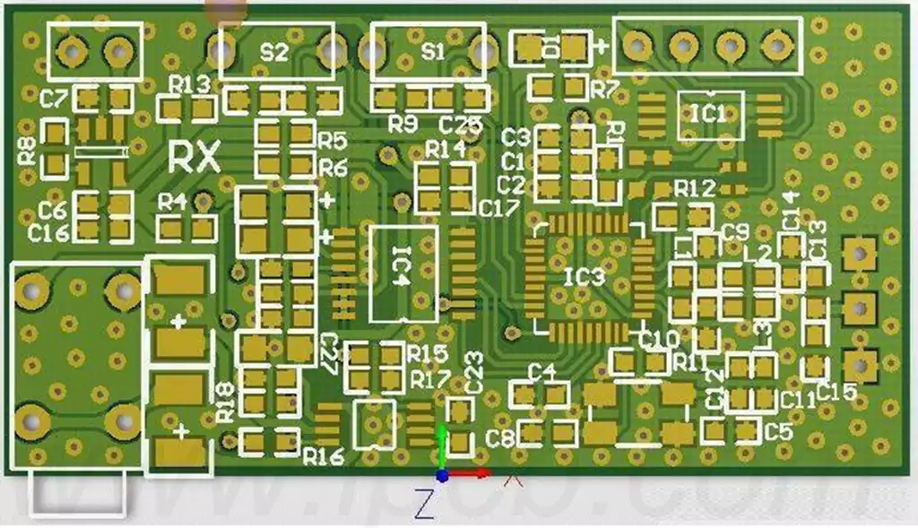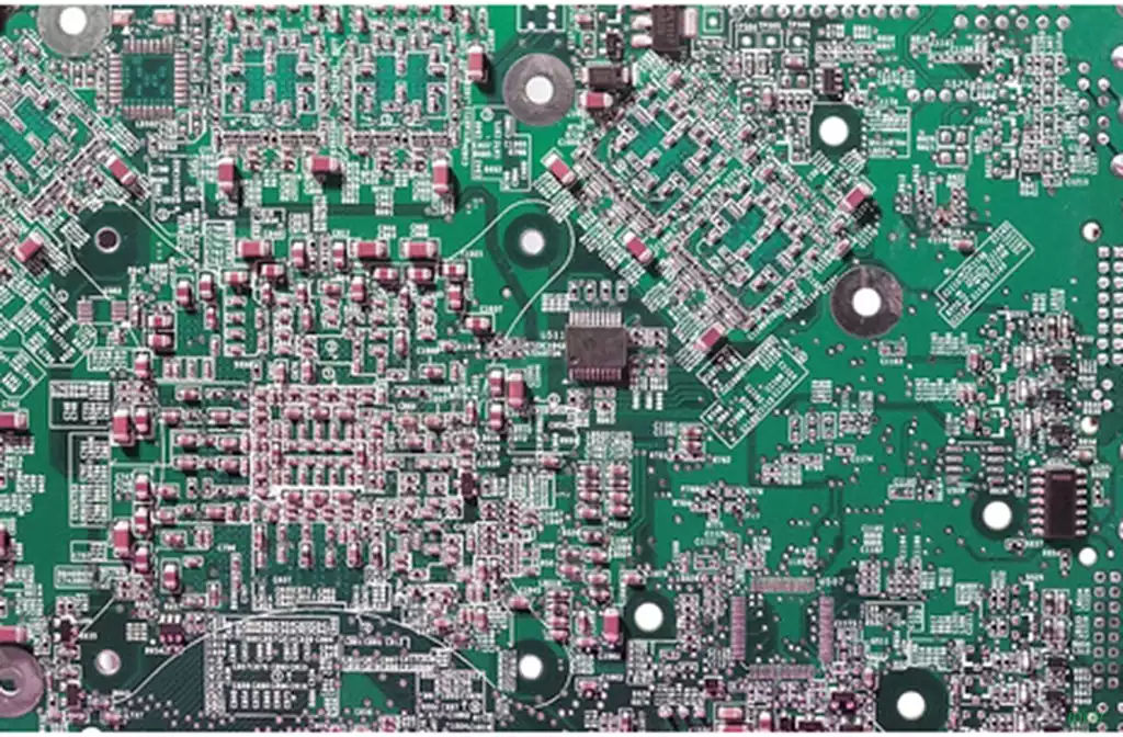
A multilayer pcb assembly combines electronic components with a printed circuit board containing three or more conductive copper layers separated by insulating materials. This construction allows engineers to route signals, distribute power, and establish ground references within a compact footprint. It is widely used in communication equipment, industrial controls, medical electronics, computing hardware, and other products that require complex circuitry.
The additional copper layers provide routing flexibility, but they also influence the board’s thermal behavior, thickness, and mechanical characteristics. These factors matter during component placement, soldering, inspection, and final testing. High component density, fine-pitch packages, large copper planes, and demanding signal-integrity requirements may require more detailed process planning than a simpler board design.
The goal of multilayer pcb assembly is not simply to install components on a densely routed board. It is to produce a complete electronic assembly that meets its electrical, mechanical, and reliability requirements consistently. Achieving this requires coordination between PCB design, component sourcing, manufacturing engineering, assembly processes, and quality control.
Preparing the PCB circuit boards and Production Files
PCB fabrication and component assembly are separate manufacturing stages. Fabrication produces the multilayer structure through processes such as inner-layer imaging, lamination, drilling, copper plating, and surface finishing. Assembly begins after the bare board has been manufactured and accepted against the applicable specifications.
Before a multilayer pcb assembly run begins, engineers review the bill of materials (BOM), component placement files, assembly drawings, PCB revision, and special manufacturing instructions. These documents must agree on component references, package types, orientations, and approved part numbers. Missing or inconsistent information can lead to incorrect placement, sourcing delays, or unnecessary production rework.
The bare pcb board also needs to meet the required dimensions, surface finish, solderability, and electrical acceptance criteria. Board thickness, copper distribution, and material selection can influence how heat spreads during soldering, so fabrication specifications should be considered alongside assembly requirements.
A design-for-manufacturing review can identify problems before production starts. Engineers should check component spacing, footprint accuracy, connector access, panelization, polarity markings, and the availability of suitable test points. For complex packages, the review should also establish whether visual inspection will be sufficient or whether X-ray inspection and specialized test equipment will be required.
The Main Stages of Multilayer PCB Assembly
The production sequence depends on the component mix, board design, and required assembly technology. A typical process may include solder paste printing, surface-mount component placement, reflow soldering, through-hole installation, selective soldering, and final inspection.
Solder paste printing and SMT placement
For surface-mount technology (SMT), solder paste is applied to the PCB pads through a stencil. Stencil thickness, aperture design, paste condition, and printing accuracy affect the volume and location of deposited solder. Too little paste can result in weak or incomplete joints, while excessive or misplaced paste can contribute to bridging and solder balls.
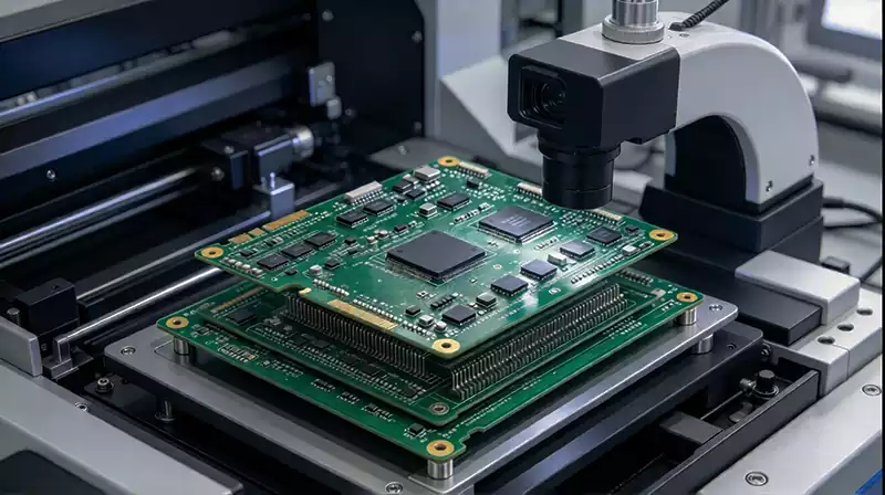
Automated pick-and-place equipment then positions components according to the approved placement data. In multilayer pcb assembly, fine-pitch integrated circuits, small passive components, connectors, and larger packages may occupy the same board. Accurate placement depends on the correct footprint, component orientation, machine programming, and reliable board alignment.
Component density can complicate assembly when parts are positioned too closely together. Insufficient spacing may interfere with stencil printing, soldering, optical inspection, or later rework. These limitations should be addressed during PCB layout rather than left entirely to the production team.
Reflow soldering and through-hole components
After SMT placement, the PCB passes through a reflow oven. The temperature profile must suit the solder paste, component specifications, and board construction. It must provide sufficient heating for proper solder wetting while keeping components and PCB materials within their permitted thermal limits.
Copper planes and thicker board constructions can affect heat distribution. Large copper areas may draw heat away from some joints, while components with different thermal masses can heat at different rates. For demanding designs, temperature profiling with thermocouples helps confirm that representative locations receive the required thermal exposure.
Through-hole components may be inserted and soldered using wave soldering, selective soldering, or manual techniques. The selected method depends on component geometry, board layout, production volume, and mechanical requirements. Connectors and other mechanically loaded parts deserve particular attention because inadequate solder coverage or weak joints can lead to intermittent connections or premature failure.
Design Factors That Influence Assembly Quality
A reliable multilayer pcb assembly depends on more than equipment accuracy. The electrical and mechanical design determines how easily the board can be assembled, inspected, and tested.
Component selection and spacing influence placement accuracy and solder-joint quality. Fine-pitch packages require compatible stencil designs and precise placement. Bottom-terminated components, including many ball grid array (BGA) packages, have hidden solder joints that cannot be fully assessed through ordinary top-side visual inspection. The inspection strategy should reflect the package type and the risk associated with potential defects.
Thermal distribution is another important factor. Large copper planes, thick boards, and uneven component sizes can create temperature differences during soldering. Engineers should review copper layout, pad geometry, component heat sensitivity, and the proposed soldering profile. Thermal behavior should be validated using the actual board and component configuration rather than assumed from oven settings alone.
Signal integrity and power delivery also require attention. Multilayer boards often use reference planes, controlled-impedance traces, and carefully planned return paths. Component substitutions, footprint changes, and assembly-related modifications should be reviewed if they could affect parasitic effects, impedance, grounding, or electromagnetic compatibility.
Mechanical considerations include board warpage, connector loading, mounting-hole alignment, and enclosure clearance. These factors are especially important for products with dense component placement or multiple board-to-board interfaces. Reviewing them early helps prevent assembly defects that may not be visible during electrical testing.
Inspection and Testing for Multilayer PCB Assembly
Inspection and testing serve different purposes, and no single method detects every possible defect. A suitable quality plan combines checks that match the board’s complexity, component packages, application, and acceptance criteria.
Solder paste inspection (SPI) measures deposited paste before component placement. Automated optical inspection (AOI) can identify visible issues such as misplaced components, polarity errors, solder bridging, and certain solder-joint defects. For BGA packages and other concealed connections, X-ray inspection may be needed to assess internal solder-joint formation.
Electrical testing provides another layer of verification. In-circuit testing (ICT), when suitable test access is available, can detect certain component and connection faults. Functional testing confirms that the completed board performs its intended tasks, such as powering up correctly, communicating with other devices, processing sensor inputs, or controlling outputs.
A complete multilayer pcb assembly quality plan should distinguish bare-board electrical testing from assembled-board testing. Bare-board testing verifies the PCB’s conductive connections before components are installed. PCB assembly testing evaluates the populated assembly and its behavior after soldering.
For products exposed to demanding operating conditions, additional qualification may be necessary. Depending on the application, this can include thermal cycling, vibration, humidity exposure, or other environmental tests. The required methods should be selected according to product specifications and reliability objectives rather than applied indiscriminately to every design.
Improving Production Yield and Long-Term Reliability
Consistent production depends on controlling the entire manufacturing workflow instead of relying on final inspection alone. Verified design files, approved components, suitable soldering profiles, stable equipment settings, and clear acceptance criteria help reduce process variation.
Component traceability can be important for complex and high-reliability products. Recording relevant component batches, inspection results, process parameters, and rework history makes it easier to investigate defects and identify recurring problems. Moisture-sensitive components and solder paste should be stored and handled according to their specified requirements.
Design-for-assembly and design-for-test reviews can further improve yield. These reviews should examine component accessibility, stencil design, panelization, test-point coverage, connector orientation, and the practicality of rework. Where a component substitution or process change is necessary, its effect on electrical performance, thermal behavior, and mechanical fit should be assessed before release.
Ultimately, successful multilayer pcb assembly requires close coordination between board design, component selection, soldering, inspection, and functional verification. When these stages are planned as one manufacturing process, engineers can reduce avoidable defects, improve production consistency, and deliver electronic products that meet their intended performance and reliability requirements.