A stencil circuit board process uses a precisely manufactured stencil to transfer solder paste onto the surface-mount pads of a printed circuit board (PCB) before component placement. Although the stencil is a separate manufacturing tool rather than part of the finished circuit board, its design directly affects solder paste volume, component alignment, solder joint formation, and overall PCBA quality. Incorrect stencil thickness or poorly designed apertures can lead to solder bridging, insufficient solder, component shifting, and open connections after reflow.
The challenge is not simply to make the stencil openings match the PCB pads. Each opening must release the correct amount of solder paste while maintaining consistent deposits across components with different package sizes and lead pitches. Fine-pitch ICs, ball grid arrays (BGAs), small passive components, and large power terminals may require different printing conditions even when they are assembled on the same board.
For reliable SMT assembly, stencil design must account for PCB pad geometry, component package requirements, solder paste properties, and the capabilities of the printing process. These factors should be evaluated before stencil fabrication rather than corrected only after assembly defects appear.
How a PCB Stencil Works in SMT Assembly
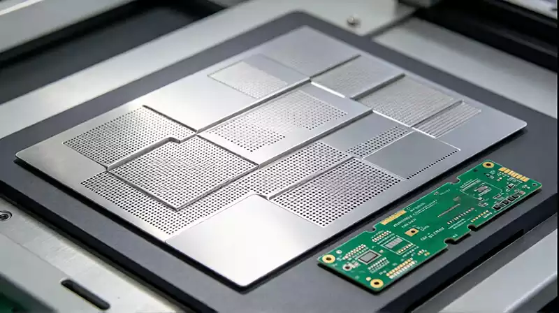
During SMT assembly, the PCB is positioned and supported beneath the stencil, and solder paste is applied across the stencil surface using a squeegee. The paste passes through the apertures and deposits onto the corresponding PCB pads. After the stencil separates from the board, the solder paste deposits remain on the pads for component placement and subsequent reflow soldering.
The quality of this transfer depends on several interacting factors. The stencil must align accurately with the PCB, the paste must fill the apertures consistently, and the aperture walls must allow the paste to release cleanly. Board warpage, inadequate support, worn stencil surfaces, or unsuitable printing parameters can all produce uneven deposits.
For example, a fine-pitch integrated circuit may have closely spaced pads that leave little room for excess solder paste. If too much paste is deposited, adjacent solder joints may bridge during reflow. If too little paste reaches the pads, the resulting joints may be weak or electrically open. A large connector pad presents a different challenge because it may require more solder volume to establish a reliable mechanical and electrical connection.
This is why stencil design should be reviewed alongside the PCB layout and assembly requirements. The stencil is part of the soldering process, and its performance depends on how well the tool, materials, and board geometry work together.
Stencil Thickness and Aperture Design
Stencil thickness determines the nominal volume of solder paste deposited through an aperture. A thicker stencil generally deposits more paste when the aperture dimensions remain unchanged, while a thinner stencil can improve paste release from small openings used for fine-pitch components.
For many SMT applications, stainless steel stencils in the approximate range of 0.10 mm to 0.20 mm are used as a starting point. Thinner options are often considered for fine-pitch packages, while thicker stencils may be appropriate for components that require larger solder deposits. These ranges are not universal specifications; the actual thickness should be selected according to the smallest apertures, component requirements, and printing process.
A common design problem occurs when a board contains both fine-pitch ICs and large connectors. A thick stencil may provide adequate paste volume for the connectors but deposit excessive paste between closely spaced IC leads. Conversely, a thin stencil may print the fine-pitch components reliably but leave insufficient solder paste on larger pads.
A step stencil can address this conflict by using different foil thicknesses in designated areas of the same tool. The thinner region supports fine-pitch printing, while the thicker region provides additional paste volume for selected components. This approach requires careful control of step locations, component clearances, and printing conditions, so it is most useful when a uniform stencil cannot meet the requirements of the entire board.
Aperture geometry is equally important. Openings should be designed around the actual PCB pad dimensions and the solder paste volume required for each component. A simple one-to-one match between the pad and aperture is not always appropriate. Fine-pitch components may need reduced or specially shaped apertures to limit bridging, while certain thermal or large-area pads may require divided openings to improve paste distribution and reduce trapped air.
The designer must also consider aperture aspect and area ratios, which describe how the opening dimensions relate to stencil thickness and the aperture walls. If an opening is too small relative to the foil thickness, solder paste may remain inside the aperture instead of transferring fully to the PCB pad. A commonly used area-ratio guideline is approximately 0.66 or higher, but this is a design reference rather than a guarantee of printing performance. Actual results depend on aperture geometry, stencil construction, paste characteristics, and process settings.
Choosing Stencil Material and Manufacturing Method
Stencil material and manufacturing quality influence aperture accuracy, surface finish, durability, and solder paste release. Stainless steel is widely used because it provides good dimensional stability and mechanical strength for repeated printing cycles.
Laser-cut stainless steel stencils are commonly used for SMT assembly because they support accurate aperture formation and can accommodate fine-pitch component layouts. Electropolishing or other suitable finishing processes can improve aperture-wall smoothness and help solder paste release more consistently.
Electroformed stencils are another option for applications requiring particularly fine features or improved paste release from challenging apertures. Their suitability depends on the required geometry, manufacturing capability, production volume, and cost.
Chemical etching may be adequate for some less demanding applications, but its process characteristics must be evaluated carefully when narrow apertures and closely spaced pads require precise control. The manufacturing method should be selected according to the board’s actual assembly requirements rather than cost alone.
Stencil condition also matters after production begins. Paste residue can accumulate on aperture walls and underside surfaces, gradually affecting transfer consistency. Damaged apertures, uneven tension, or poor stencil flatness may create localized printing defects. Regular cleaning, inspection, and process monitoring help maintain consistent results across repeated production runs.
Preventing Solder Paste Printing Defects
Many SMT soldering problems originate during solder paste printing, even when they become visible only after reflow. Identifying the relationship between the defect and the stencil helps engineers correct the underlying cause instead of repeatedly adjusting unrelated assembly parameters.
Solder bridging occurs when solder connects adjacent pads or leads that should remain electrically separate. Excessive paste volume, apertures that are too large, poor stencil-to-board contact, or inaccurate alignment can contribute to bridging. For fine-pitch ICs, controlled aperture reduction and consistent stencil alignment can help reduce the risk.
Insufficient solder paste can produce weak joints, open connections, or inadequate solder coverage. Possible causes include apertures that are too small, poor paste release, clogged openings, unsuitable paste particle size, and inconsistent printing conditions. Engineers should inspect the aperture design and stencil cleanliness before assuming that the problem originates in the reflow process.
Uneven deposits can result from poor PCB support, board warpage, inconsistent squeegee pressure, or variations in stencil separation. If the PCB does not remain sufficiently flat against the stencil during printing, paste may spread beneath the foil or transfer unevenly between pads.
Solder paste inspection (SPI) provides a way to evaluate deposit volume, height, area, and position before components are placed. When inspection identifies repeated defects at particular pads, the results can guide targeted changes to aperture dimensions, stencil thickness, alignment, or printing parameters.
The key is to distinguish between a design limitation and a process problem. Repeated defects at the same component locations may indicate unsuitable aperture geometry, while inconsistent defects across different locations may point toward paste condition, stencil cleanliness, board support, or printer setup.
Stencil Design for Fine-Pitch and High-Density PCBs
Fine-pitch packages and high-density PCB layouts require tighter control of solder paste deposition because the available spacing between adjacent pads is limited. Components such as QFNs, BGAs, CSPs, and small passive devices may have openings that are difficult to print consistently with a standard stencil thickness.
For these applications, engineers should review the smallest aperture dimensions, stencil thickness, paste particle size, and expected transfer performance together. Reducing stencil thickness can improve paste release, but it also reduces the amount of solder deposited. Aperture modifications may help, but excessive reduction can result in insufficient solder and unreliable joints.
BGA assembly requires particular attention to the relationship between ball size, PCB pad geometry, aperture design, and solder paste volume. Inadequate or inconsistent deposits can contribute to open joints, while excessive deposits may increase the risk of solder bridging between adjacent connections. The appropriate design must be based on the specific package and assembly process.
Thermal pads beneath power components and QFNs present a different challenge. A single large aperture can trap gas released during reflow and contribute to voiding. Dividing the opening into smaller sections can improve paste distribution and provide pathways for gas escape, although the final pattern must be validated against the component manufacturer’s recommendations and thermal requirements.
When the board contains a mixture of fine-pitch devices, large connectors, and thermal pads, the stencil should be optimized for the complete component layout. Designing each aperture independently without considering neighboring components and overall paste distribution can create conflicting requirements across the board.
Integrating Stencil Requirements Into PCB Assembly
Stencil design should begin before the PCB enters production. The assembly team needs accurate PCB fabrication data, component footprints, solder paste specifications, and any package-specific soldering recommendations. Changes to pad dimensions or component selection should trigger a review of the corresponding stencil apertures.
For prototype builds, a design review and initial print inspection can reveal problems before larger quantities are assembled. This is particularly useful for boards with fine-pitch components, small passive devices, or unusual thermal-pad geometries. Early adjustments can reduce repeated rework and prevent the same printing defect from carrying into mass production.
For volume manufacturing, repeatability becomes just as important as initial print quality. The stencil must maintain its dimensional accuracy, and the printing process must deliver consistent paste deposits across boards and production batches. SPI data, stencil cleaning records, alignment checks, and defect analysis can help identify process drift before it affects a significant number of assemblies.
Stencil requirements should also be coordinated with the PCB assembly provider when a board has unusual pad patterns or demanding component packages. Reviewing the design before fabrication helps determine whether the selected thickness, aperture geometry, and manufacturing method are practical for the intended assembly process.
Building a Reliable Stencil Circuit Board Process
A reliable stencil circuit board process requires coordination between PCB layout, stencil fabrication, solder paste selection, and SMT printing. Engineers should begin by identifying the components with the most demanding paste-volume requirements, then select stencil thickness and aperture geometry that accommodate those constraints without compromising the remaining components.
Before production, verify aperture dimensions, stencil alignment, board support, and paste compatibility. During assembly, monitor deposit quality through visual inspection or SPI, and investigate repeated defects at their source. After reflow, confirm that the solder joints meet the electrical, mechanical, and reliability requirements of the finished assembly.
The objective is not simply to produce a stencil that matches a PCB drawing. It is to achieve consistent solder paste transfer across different pad sizes and component packages. By treating stencil design as an integral part of the PCB assembly process, manufacturers can reduce printing defects, improve solder joint consistency, and support more dependable PCBA production.