In the grand panorama of modern global industrial automation, from the tireless heavy-duty CNC machine tools and crisscrossing intelligent logistics sorting lines to the underground oil drilling equipment and the high-flying wind power converters, countless complex electronic control systems silently support the physical operation of human civilization. Hidden within these high-load, high-risk devices are circuit boards that have undergone rigorous testing and refinement—these are industrial-grade printed circuit boards (PCBs).
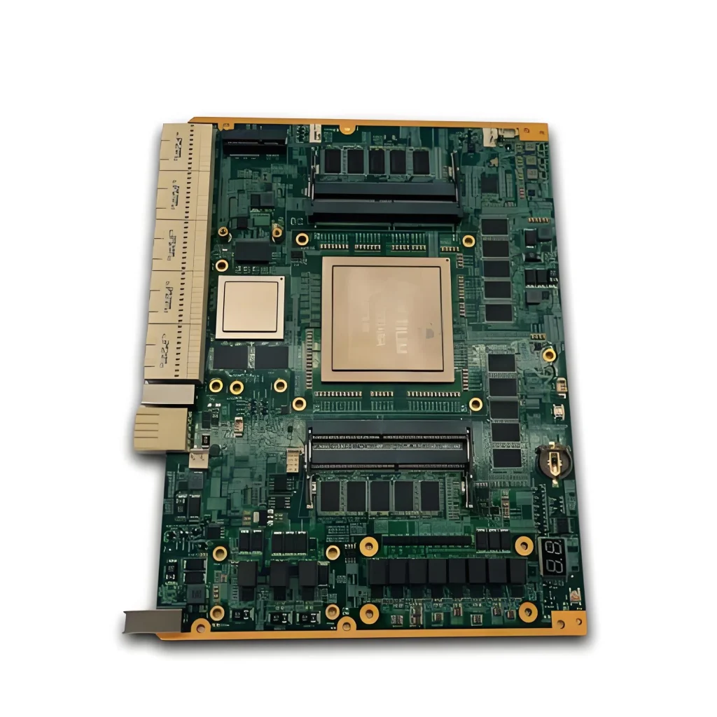
Unlike consumer electronics circuit boards (such as smartphone or laptop motherboards) that prioritize thinness, size, and rapid product updates, industrial-grade PCBs are the true “steel backbone of industry.” Their design philosophy does not pursue momentary brilliance, but rather prioritizes ultimate reliability under extreme environments, continuous operating life of ten or even decades (24/7/365), and absolute control over high voltage and high current. In industrial settings, even a minor circuit board failure can paralyze an entire production line, result in millions of dollars in economic losses, and even trigger a major industrial safety accident.
This article will meticulously analyze and guide you through the underlying technological logic and manufacturing evolution of industrial PCB in areas such as materials science, harsh environment protection, high-current thermodynamic topology, and extreme reliability testing engineering.
The Physical Divide Between Consumer and Industrial Grades
To understand why industrial-grade PCBs have such stringent design standards, we must first be keenly aware of the harsh physical world they face. Consumer electronics typically thrive in comfortable, moderately humid, dust-free, and stable office or home environments; industrial PCBs, on the other hand, must directly confront the multiple physical pressures posed by nature and heavy industrial environments.
The Thermal Shock of Extreme Temperature Fluctuations
The temperature environment in industrial settings often exhibits extreme polarization or drastic fluctuations. For example, the control board inside a solar photovoltaic inverter installed in a desert region may experience internal temperatures soaring to over 80 degrees Celsius under intense sunlight; while automated equipment installed in high-altitude outdoor communication base stations or in cold regions needs to start instantly in freezing environments of minus 40 degrees Celsius. This intense alternation of hot and cold temperatures generates continuous mechanical thermal stress on the circuit board.
Mechanical Vibration and High-Frequency Impact: Circuit boards inside heavy machinery, engineering vehicles, rail transportation, and industrial robots are constantly subjected to high-frequency vibrations and continuous mechanical impacts. The roar of engines, the rapid stops of robotic arms, and the intense pressing of punch presses are all directly transmitted to the circuit board through the chassis. If the mechanical structure and solder joints of the circuit board are poorly designed, long-term micro-vibration can lead to metal fatigue, eventually causing solder joint cracking or lead wire breakage.
Chemical Corrosion, High Humidity, and Salt Spray Erosion: In chemical plants, sewage treatment plants, marine vessels, or coastal industrial areas, the air is filled with large amounts of hydrogen sulfide, chlorine, high concentrations of salt spray, and industrial acid and alkaline waste gases. These highly corrosive chemicals, upon contact with exposed copper foil or solder joints on the circuit board surface, rapidly trigger electrochemical corrosion, causing the conductors to be silently “eaten away” or forming conductive salt crystals between different potentials, resulting in catastrophic short circuits.
Electromagnetic Interference (EMI) and High-Voltage Surge Impact
Industrial environments are filled with various high-power motors, frequency converters, high-power relays, and welding machines. These devices release extremely strong electromagnetic pulses (EMPs) and high-voltage surges into space and the power grid during switching. Industrial-grade PCBs must possess extremely strong electromagnetic interference resistance while protecting their sensitive logic chips from instantaneous high-voltage breakdown.
A Genetic Leap in Basic Materials: High Tg Resin and Heavy Copper Foil Engineering
To physically resist the corrosive effects of these harsh environments, industrial-grade printed circuit boards differ significantly from consumer-grade circuit boards from the very first step in their manufacturing process—the selection of basic materials.
Applications of High-Tg Epoxy Resin Substrates
Consumer-grade circuit boards typically use standard epoxy resin fiberglass cloth substrates (such as common FR-4), with a glass transition temperature (Tg) usually around 130 degrees Celsius. When the temperature exceeds this critical point, the resin matrix begins to transition from a hard glassy state to a soft rubbery state, resulting in a precipitous drop in mechanical strength and a sharp increase in the coefficient of thermal expansion (CTE).
In industrial-grade PCBs, high-Tg epoxy resin substrates (Tg reaching 170 degrees Celsius or even higher) are the industry standard. High-Tg materials possess a denser cross-linked molecular network structure, meaning they maintain extremely high dimensional stability when facing high temperatures, thermal shock, and multiple reflow soldering operations. This significantly suppresses excessive expansion in the Z-axis direction, thus protecting internal plated vias (PTHs) from breakage.
Heavy Copper Foil and High-Current Carrying Structures
Industrial control boards often need to drive high-power motors, solenoid valves, or actuators, with currents flowing through the circuit boards often reaching tens or even hundreds of amperes. Traditional 35-micron thick copper foil (one ounce of copper) would burn out instantly due to excessive Joule heating when faced with such a large operating current.
Therefore, industrial-grade PCBs widely employ heavy copper foil technology. Engineers increase the copper foil thickness to 70 microns (two ounces), 105 microns (three ounces), and even hundreds of microns thick in extremely high-current power boards. The thick copper foil not only smoothly carries the powerful current, reducing the DC resistance and heat generation of the circuitry, but also rapidly conducts localized heat sources away on a flat surface, acting as an excellent heat dissipation channel.
Microscopic Protection and Hardening: Conformal Coating, Encapsulation, and Isolation Barriers
After selecting a robust substrate and thick copper foil, completely isolating the circuit board from the harsh external environment is another core battle in industrial-grade PCB design.
The Molecular Barrier of Conformal Coating
To combat moisture, salt spray, and chemical corrosion, most industrial-grade PCBs are uniformly sprayed or dipped with a layer of conformal coating after surface mounting and soldering.
Depending on their chemical composition, conformal coatings are mainly classified as acrylic resin, silicone resin, polyurethane resin, and Parylene vapor deposition coating. This transparent protective film adheres tightly to the surface of every component and the gaps in the traces on the circuit board, like skin. It perfectly blocks the penetration of water molecules, dust, and corrosive gases. Parylene coatings, in particular, through vacuum pyrolysis vapor deposition technology, can generate a completely pinhole-free, uniformly thick nanoscale polymer crystal film at the microscale, providing the industry’s top-tier chemical and moisture protection.
Potting & Encapsulation and Mechanical Vibration Resistance
For industrial modules deployed in outdoor, automotive, or high-vibration environments (such as automotive sensors or outdoor power modules), a thin layer of conformal coating is insufficient. The manufacturer employs a potting process.
The entire circuit board, along with its casing, is placed in a specialized mold, and then liquid two-component epoxy, polyurethane, or silicone potting compound is injected until the entire internal space is completely filled and then heated to cure. The cured potting compound forms a robust, solid protective block. This not only completely isolates the circuit from air and moisture but also securely holds all electronic components in place, preventing pin fatigue or component loosening from mechanical vibrations or impacts from any direction. Simultaneously, the potting compound possesses excellent thermal conductivity, efficiently transferring heat from densely packed heat-generating components to the casing.
Physical Isolation of High-Voltage Electrical Clearances and Creepage Distances
In industrial power control and frequency converter drive PCBs, low-voltage digital logic circuits and high-voltage circuits of several kilovolts often coexist. To prevent high-voltage arcing through air (insufficient electrical clearances) or creepage breakdown along insulating surfaces (insufficient creepage distances), industrial-grade PCB topology design adheres to near-stringent geometric red lines.
Engineers must ensure sufficient physical spacing between high- and low-voltage traces at different potentials, based on operating voltage levels, pollution levels, and insulation material types. For space-constrained boards, “slotting” grooves are milled directly into the circuit board using a CNC milling machine. Air’s insulation strength is far lower than that of solid substrates; milling these slots lengthens the physical path of electric arcs, fundamentally preventing the catastrophic short circuit caused by high-voltage arcing.
Strict Electromagnetic Compatibility (EMC) and Interference Immunity
Industrial environments are complex electromagnetic spaces rife with electromagnetic interference. High-frequency chopping by inverters and the starting and stopping of high-power motors generate massive amounts of conducted and radiated interference. Without in-depth EMC design, industrial-grade PCBs will frequently experience data loss, malfunctions, and even system crashes.
Shielding Matrix for Ground and Power Planes on Multilayer Boards
In high-end industrial control boards, double-sided boards are no longer sufficient for interference immunity; multilayer board architectures have become standard.
By scientifically planning the layered structure, a dedicated continuous ground plane is tightly sandwiched between the high-speed signal layer and the power layer, forming a natural electromagnetic shield. This continuous ground plane not only provides a low-impedance return path for high-frequency signals but also acts like an impenetrable Faraday net, reflecting or absorbing external electromagnetic radiation on the outer layer, protecting the sensitive internal microcontroller from interference.
Transient Suppression and Multi-Level Surge Protection Network
To cope with lightning surges and electrostatic discharge (ESD) from power ports or external sensor signal lines, industrial-grade PCBs must construct multi-level protection at their input/output (I/O) interfaces.
Engineers precisely place gas discharge tubes (GDTs), transient voltage suppressor diodes (TVS), and varistors (MOVs) at the interface front-end. These protective devices are always ready with extremely fast response times (nanosecond levels). When a high-voltage surge occurs, they instantly conduct, directly dissipating thousands of volts of dangerous high-voltage energy to the chassis ground plane, ensuring the delicate digital circuitry at the back end remains undamaged.
The Ultimate Judge of Industrial Quality: Accelerated Life Testing and Environmental Stress Screening
A perfect industrial-grade PCB not only strives for excellence in its design but also undergoes a series of brutal physical tests at the final stage of manufacturing to earn its place in the industrial market.
High-Temperature Aging and Environmental Stress Screening (ESS)
Before mass production, industrial-grade electronic modules are typically placed in a high-temperature aging room. Under high temperatures (usually around 85 degrees Celsius) and full load operation, the circuit board needs to run continuously for tens or even hundreds of hours.
This test is scientifically based on the “bathtub curve” in reliability engineering. Early failures of electronic components (such as hidden solder joints, inferior chips, and microcracks) often occur in the initial stages of power-on. Accelerated aging screening at the factory exposes and eliminates these potential early defects before shipment, ensuring that every industrial PCB delivered to the customer has passed its infancy and entered a stable period lasting several years.
High Accelerated Life Testing (HALT) and High Accelerated Stress Audit (HASA)
During the R&D design phase, to explore the physical limits of industrial PCBs, engineers conduct destructive High Accelerated Life Testing (HALT).
The circuit board is fixed in a combined vibration table and a rapid temperature change chamber. Testers apply extreme high and low temperature alternating stresses and six-axis random mechanical vibrations at rates far exceeding the product’s nominal limits until the circuit board exposes weaknesses in its physical structure (such as fatigue fracture at a solder joint or overheating failure of a chip). Through this extreme testing, engineers can identify design blind spots in advance, improve the structural topology, and thus push the robustness of industrial PCBs to its absolute peak.
Conclusion: The Silent Foundation Behind Industrial Civilization
Industrial-grade printed circuit boards (PCBs) are the most understated yet indispensable silent foundation of modern industrial civilization. They lack the dazzling appearance and vibrant screens of consumer electronics, yet they steadfastly uphold their promise of zero defects day after day in an extreme world of cold, vibration, corrosion, and high pressure.
From selecting high-Tg heat-resistant substrates and heavy copper foil high-current topologies, to the molecular-level chemical defenses constructed with conformal coatings and potting compounds; from multi-layered electromagnetic shielding to the rigorous selection process of undergoing fiery baptism in high-temperature aging chambers, every tiny detail of industrial-grade PCBs profoundly interprets meticulous engineering thinking and the ultimate pursuit of reliability. It is thanks to these steel-like circuit boards silently supporting us behind the scenes that human intelligent manufacturing, energy revolution, and modern industrial automation can steadily move forward amidst storms and sail towards a broader future.