If you are searching what is a PCBA board, the direct answer is that it is a printed circuit board after electronic components have been mounted and electrically connected. A bare PCB provides copper conductors, pads, vias and mechanical support, while a PCBA performs the intended electronic function.
The complete answer to what is a PCBA board also involves understanding how a bare board becomes a working electronic assembly. Solder-paste printing, component placement, reflow soldering, inspection, programming and functional testing all influence whether the finished PCBA operates reliably.
What PCBA Actually Means
PCBA stands for printed circuit board assembly. Technically, the phrase “PCBA board” repeats the word “board,” because the final letter in PCBA already represents assembly rather than board. However, “PCBA board” is widely used by buyers and engineers when referring to an assembled circuit board.
To answer what is a PCBA board accurately, it is useful to distinguish three related terms:
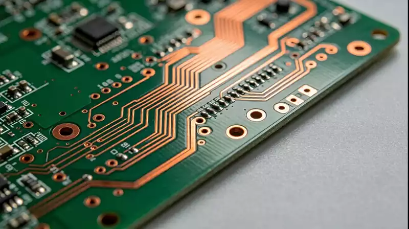
A PCB is the unpopulated board containing the insulating substrate, copper circuitry, plated holes, solder mask and surface finish. A PCBA is that PCB after components have been installed and soldered. The complete electronic product may include the PCBA together with an enclosure, cables, display, battery, sensors and other mechanical parts.
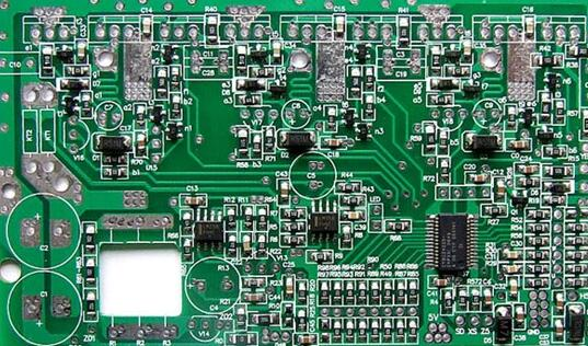
IPC terminology defines a printed board assembly as an assembly that uses a printed board for component mounting and electrical interconnection.
The Difference Between PCB and PCBA
People asking what is a PCBA board are often trying to understand whether a PCB quotation includes components and assembly. This distinction matters because PCB fabrication and PCBA manufacturing are different production stages.
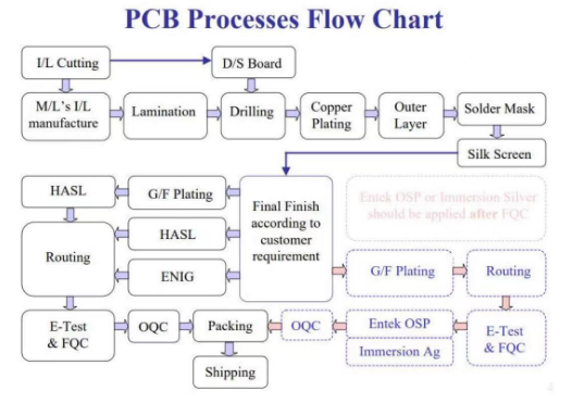
PCB fabrication begins with copper-clad laminate. The manufacturer forms the circuit pattern, drills holes, plates copper, laminates multilayer structures, applies solder mask and creates the required surface finish. The delivered product is still a passive interconnection structure.
PCBA manufacturing begins with the finished bare PCB. Components specified in the bill of materials are sourced, inspected, placed and soldered to the board. The assembly may then receive firmware, electrical testing, conformal coating or final product integration.
A bare PCB may pass continuity testing but still cannot perform the product’s function. The PCBA becomes operational only after the correct components and software are combined with the board.
How a Bare PCB Becomes a PCBA
A complete explanation of what is a PCBA board must include the manufacturing process because many assembly defects are created by interactions between several operations rather than by one isolated machine.
Solder Paste Printing Establishes Joint Volume
For surface-mount assembly, a stainless-steel stencil aligns with the PCB pads. A squeegee moves solder paste across the stencil so that paste passes through each aperture and deposits on the exposed pads.
The deposited volume affects the finished solder joint. Too little paste can create weak or open connections, while excessive or uneven paste increases the risk of bridging, solder balls and component movement during reflow.
Stencil thickness and aperture geometry should match the component mix. A board containing fine-pitch integrated circuits, large power components and very small passive devices may require localized aperture adjustments because one uniform opening strategy will not suit every joint.
Solder-paste inspection measures deposit position, area, height and volume before components are placed. Detecting a printing problem at this stage prevents the same error from affecting an entire production panel.
Placement Accuracy Depends on More Than Machine Speed
Pick-and-place equipment identifies components, checks their orientation and positions them on the printed solder paste. Feeders, camera systems, fiducials and placement programs must all correspond to the approved component and PCB revision.
Understanding what is a PCBA board therefore includes understanding the BOM and placement data. A machine can place a component with high positional accuracy while still installing the wrong value or package if the feeder setup or source data is incorrect.
Package markings, polarity indicators and reference designators should remain unambiguous. Diodes, electrolytic capacitors, LEDs and integrated circuits can be physically mounted in the correct location but electrically reversed.
Component substitutions require engineering control. Two devices with matching package dimensions may differ in pin assignment, thermal behaviour, firmware compatibility or electrical performance.
Reflow Creates the Metallurgical Connection
After placement, the assembly travels through a reflow oven. The temperature profile warms the PCB, activates the solder-paste flux, melts the alloy and then cools the solder to form electrical and mechanical connections.
For anyone researching what is a PCBA board, reflow is the stage that converts positioned components into permanently connected circuitry. The profile must provide enough energy for soldering without exceeding the limits of the board or components.
Large copper areas and power components heat differently from small pads and passive devices. An unsuitable profile may produce incomplete wetting, voids, tombstoning or thermal damage. The correct settings depend on board thickness, copper distribution, component mass, solder paste and oven performance.
A profile should be measured on a representative assembly rather than selected only from the solder-paste datasheet. Thermocouples placed near thermally different components reveal whether every important joint experiences an acceptable process window.
Through-hole components may be installed by wave soldering, selective soldering or manual soldering after SMT reflow. Mixed-technology assemblies therefore require additional process planning.
Inspection Does Not Replace Functional Testing
The question what is a PCBA board is not fully answered when assembly ends at soldering. The finished board must also be inspected and tested.
Automatic optical inspection can identify missing components, polarity errors, placement shifts and many visible solder defects. It cannot directly inspect solder joints hidden beneath BGA, LGA and other bottom-terminated packages. X-ray inspection is used where internal solder distribution, bridging or voiding must be evaluated.
IPC-A-610 provides visual acceptability requirements for electronic assemblies, while J-STD-001 defines material, process and acceptance requirements for soldered assemblies. The required product class and customer-specific criteria should be agreed before manufacturing begins.
A visually acceptable solder joint does not prove that the complete circuit works. Inspection must therefore be followed by the appropriate electrical and functional tests.
PCBA Testing Confirms the Board Can Perform Its Function
A practical answer to what is a PCBA board must include test coverage. Testing determines whether assembled components, solder joints, firmware and interfaces operate together as intended.
In-circuit testing can measure selected components and electrical networks through test probes. Flying-probe testing provides flexibility for prototypes and smaller batches because it does not require a dedicated bed-of-nails fixture. Functional testing powers the assembly and checks its actual inputs, outputs and operating behaviour.
The test method should match the product. A power controller may require load testing and protection checks. A wireless device may require programming and communication verification. A sensor board may need calibrated input signals instead of a simple power-on test.
Test access must be considered during PCB design. Ground, programming, reset, communication and important power rails should remain accessible. Removing every test pad to reduce board size can increase fixture complexity and make production failures difficult to diagnose.
A PCBA Is Defined by Its Manufacturing Data
When buyers ask what is a PCBA board, they should also understand that the physical assembly is controlled by several connected data files.
The Gerber or ODB++ package defines the PCB. The bill of materials identifies the approved components, while centroid data controls placement position and rotation. Assembly drawings communicate polarity and special installation requirements. Firmware and test procedures determine how the completed board is programmed and verified.
These files must describe the same revision. A current PCB combined with an outdated BOM or placement file may create an assembly that looks correct but cannot operate. Revision control is therefore part of PCBA quality, not merely document management.
PCBA Quality Depends on the Intended Application
The answer to what is a PCBA board changes very little across industries, but the required manufacturing controls can differ considerably. A low-cost consumer device and an industrial safety controller may use similar assembly processes while requiring different inspection, traceability and environmental testing.
Product requirements determine acceptable materials, soldering criteria, cleanliness, coating, component traceability and test coverage. Reliability cannot be judged only from whether the board powers on after assembly.
At iPCB, customers asking what is a PCBA board can obtain support covering PCB fabrication, component sourcing, SMT and through-hole assembly, inspection, programming and functional testing. Keeping these stages within one controlled manufacturing workflow helps maintain consistency between the design data and finished assembly.
What Information Is Needed for a PCBA Quotation
For procurement teams searching what is a PCBA board, a complete quotation package normally requires more than Gerber files. The manufacturer needs the BOM, placement data, assembly drawings, required quantity and testing requirements.
The quotation should clarify whether components will be supplied by the customer or sourced by the manufacturer. It should also identify approved substitutions, programming requirements, special inspection, conformal coating and final assembly services.
Providing this information early allows the manufacturer to evaluate both technical feasibility and actual production cost. A PCB price alone does not represent the cost of a finished PCBA.
From Passive Board to Functional Electronics
Ultimately, what is a PCBA board can be answered by the transformation it represents. The PCB begins as a passive structure containing copper connections. Assembly adds the components, solder joints and programmed functions required to make that structure perform useful electronic work.
Understanding what is a PCBA board means recognizing that its reliability comes from more than the bare board or individual components. Data consistency, solder-paste control, placement accuracy, reflow, inspection and functional testing must work together to produce a repeatable electronic assembly.