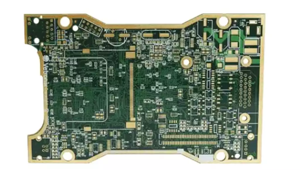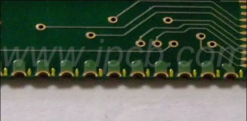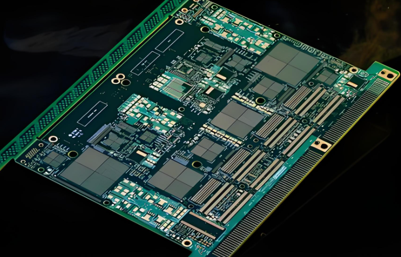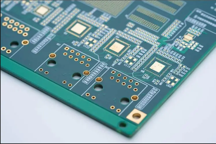
PCB board fabrication is the process of converting an electronic circuit design into a physical printed circuit board that can support components and provide reliable electrical connections. It involves several manufacturing operations, including material preparation, circuit imaging, copper etching, drilling, plating, lamination, and surface finishing. Each operation must meet specific design requirements because even small variations in copper thickness, hole positioning, or layer alignment can affect the performance of the finished board.
Printed circuit boards are used in almost every area of modern electronics, from household appliances and industrial control equipment to automotive systems, medical devices, and telecommunications products. Although these applications have different electrical and mechanical requirements, they all depend on a PCB structure that provides stable connections and sufficient durability throughout the product’s service life.
Understanding how a circuit board is manufactured helps engineers make more practical design decisions before production begins. It also gives purchasing teams a better basis for evaluating suppliers, comparing manufacturing quotations, and identifying potential quality risks.
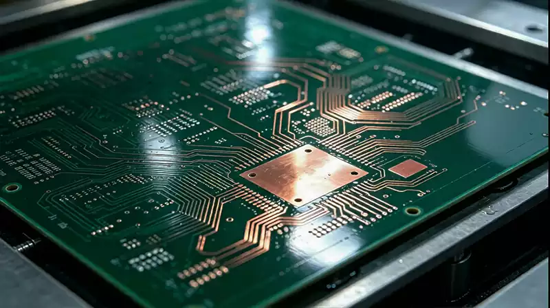
A printed circuit board consists of conductive copper patterns supported by an electrically insulating substrate. These copper patterns connect electronic components through carefully designed pathways, while the insulating material separates different conductive areas and provides mechanical stability.
The structure of a PCB varies according to its layer count and intended application. A simple board may contain copper on only one side of the substrate, whereas a multilayer design uses several copper layers separated by insulating materials. More advanced structures may also include blind vias, buried vias, microvias, or specialized dielectric materials to support compact layouts and high-speed signals.
Most conventional rigid PCBs contain four basic structural elements.
Substrate and Copper Layers
The substrate provides the mechanical foundation of the board and electrically isolates the conductive circuits. FR-4 is one of the most widely used materials because its glass-fiber reinforcement and epoxy resin offer a suitable combination of mechanical strength, electrical insulation, and thermal performance.
Copper foil is bonded to the substrate to form the conductive layers. The copper thickness is selected according to current requirements, trace dimensions, and the electrical characteristics of the design. Standard copper weights are commonly used for general electronic applications, while power electronics and other demanding applications may require heavier copper.
Solder Mask and Silkscreen
The solder mask is a protective coating applied over the outer copper layers, leaving openings where soldering or electrical contact is required. It helps reduce the risk of solder bridging and protects exposed copper from oxidation and contamination during handling.
Silkscreen markings are printed on the board to identify component positions, reference designators, polarity, logos, and other manufacturing information. These markings make the board easier to assemble, inspect, and maintain, particularly when the circuit contains many components.
How the PCB Board Fabrication Process Works
PCB Design Review and Manufacturing Preparation
Before production starts, the manufacturer reviews the engineering files to confirm that the board can be manufactured according to the specified requirements. Typical production data includes Gerber files or ODB++ files, Excellon drill files, board dimensions, stackup information, copper thickness, and surface finish specifications.
The engineering team usually performs a Design for Manufacturability review to identify problems that could affect production. Trace width and spacing, annular ring dimensions, drill sizes, copper-to-edge clearance, and solder mask openings are among the details that need to be checked.
In real production, some design problems are not immediately obvious in the layout software. For example, a narrow annular ring may meet the design rule settings but leave insufficient manufacturing tolerance after drilling and plating. Reviewing these details before fabrication can reduce the need for engineering changes and help prevent unnecessary production delays.
Material Selection and Inner Layer Production
Once the design has been approved, the manufacturer prepares the laminate and copper-clad materials required for the specified board structure. Standard FR-4 is suitable for many general-purpose applications, but specialized products may require high-Tg laminates, high-frequency materials, polyimide, or metal-core substrates.
For multilayer boards, the inner copper layers are processed before the complete stackup is assembled. A photoresist coating is applied to the copper surface, and the circuit image is transferred through UV exposure or laser direct imaging. After development, chemical etching removes unwanted copper and leaves the required conductive patterns.
Automated optical inspection is commonly used to compare the finished copper patterns with the original design data. This inspection can identify missing connections, unwanted copper, short circuits, and other defects before the inner layers become enclosed within the finished board.
Multilayer Lamination and Layer Alignment
Multilayer PCB fabrication requires individual copper layers to be bonded together into a single structure. The patterned inner layers are arranged according to the specified stackup, with prepreg materials placed between them to provide electrical insulation and bonding.
The assembled layers are exposed to controlled temperature and pressure in a lamination press. During this operation, the resin in the prepreg softens and flows before curing, creating a solid structure that holds the copper layers together.
Layer alignment needs to be controlled throughout this process because misregistration can affect via connections and the available copper area around drilled holes. As the number of layers increases, maintaining consistent registration and dielectric thickness becomes more demanding.
For high-speed circuit boards, the stackup also needs to be considered from an electrical perspective. Dielectric thickness, material properties, copper distribution, and reference plane placement can all influence impedance and signal integrity.
Drilling and Copper Plating
After lamination, holes are drilled according to the manufacturing data. Mechanical drilling is commonly used for standard through-holes and many conventional vias, while laser drilling is often applied to small microvias in high-density interconnect boards.
The drilling process must produce clean and accurately positioned holes because the hole walls will later become part of the electrical connection between copper layers. Residual resin and drilling debris are removed through desmear and hole-wall preparation before the plating process begins.
Electroless copper is deposited onto the prepared hole walls to create an initial conductive layer. Electrolytic copper plating then increases the copper thickness to the required specification. This process allows plated through-holes and vias to connect different conductive layers within the PCB.
Poor hole-wall preparation, uneven plating, or incorrect drilling conditions can cause defects such as insufficient copper coverage and weak interlayer connections. These problems may not be visible from the board surface, which is why plating control and appropriate inspection methods are important.
Outer Layer Patterning and Etching
Once the drilling and initial metallization operations are complete, the outer copper layers are processed to form the final circuit patterns. Photoresist imaging defines the areas that need to retain copper, while plating and etching operations create the required traces, pads, and conductive areas.
The manufacturing method must account for the relationship between trace width, copper thickness, and etching characteristics. When the design contains fine lines or narrow spacing, small variations during imaging and etching can have a noticeable effect on the finished circuit geometry.
After pattern formation, inspection equipment checks the outer layers for open circuits, unwanted copper connections, and other pattern defects. This stage helps ensure that the fabricated copper structure matches the original design.
Solder Mask Application and Surface Finishing
The outer copper patterns are covered with solder mask to protect the circuitry and expose only the areas required for soldering or electrical contact. The coating is applied and processed according to the manufacturer’s production method, with openings created for component pads, test points, and other specified features.
After solder mask curing, silkscreen information is printed where required. The board then receives a surface finish to protect exposed copper and provide a suitable contact surface for component assembly.
Common PCB surface finishes include HASL, lead-free HASL, ENIG, OSP, and immersion silver. Each option has different characteristics in terms of surface flatness, solderability, storage requirements, and manufacturing cost.
For example, ENIG is often selected for fine-pitch components because it provides a relatively flat surface. HASL remains a practical option for many general-purpose boards where cost is an important consideration and pad flatness is less demanding.
The selection should be based on the actual assembly process and product requirements rather than choosing a finish simply because it is widely used.
Board Profiling and Electrical Testing
The final manufacturing operations include separating individual boards from the production panel and checking whether the finished circuits meet the specified requirements. CNC routing and V-scoring are commonly used for board separation, depending on the PCB design and assembly needs.
Electrical testing is performed to identify unintended shorts and open circuits. Flying probe testing is often used for prototypes and smaller production runs because it does not require a dedicated test fixture. Fixture-based testing is generally more suitable for larger production quantities where repeated testing can justify the initial fixture cost.
Depending on the board specifications, the manufacturer may also carry out dimensional inspection, automated optical inspection, microsection analysis, and controlled impedance testing. These checks provide additional information about the quality of the finished board and its suitability for the intended application.
Common PCB Types and Their Manufacturing Requirements
The construction of a PCB has a direct effect on its manufacturing process. Selecting the appropriate board type requires consideration of circuit complexity, available space, operating conditions, and electrical performance.
Single Layer and Double Layer PCBs
Single-layer PCBs contain copper circuitry on one side of the insulating substrate. Their relatively simple structure makes them suitable for basic electronic products, LED lighting, power supplies, and circuits that do not require extensive routing.
Double-layer PCBs have conductive copper on both sides of the substrate, with plated through-holes providing connections between the layers. This arrangement gives designers greater routing flexibility without the additional lamination operations required for multilayer boards.
Both types are widely used in electronic products where manufacturing cost, straightforward assembly, and practical circuit density are important considerations.
Multilayer PCB Manufacturing
Multilayer boards contain three or more conductive copper layers separated by insulating materials. They allow more complex circuits to fit within a limited board area and provide additional options for power distribution, grounding, and signal routing.
A four-layer PCB, for example, may use dedicated ground and power planes to improve circuit layout and reduce unwanted electromagnetic coupling. Boards with higher layer counts are common in communication equipment, computing hardware, industrial control systems, and other products with demanding electrical requirements.
However, increasing the layer count also introduces additional manufacturing considerations. Lamination accuracy, layer registration, dielectric thickness, via design, and impedance control all need to be evaluated during engineering preparation.
HDI and Rigid Flex PCBs
High-density interconnect PCBs use finer traces, smaller vias, and more compact connection structures to accommodate high component density. Laser-drilled microvias and sequential lamination are commonly used in HDI manufacturing, making process control more demanding than in conventional rigid PCB production.
Rigid-flex PCBs combine rigid circuit sections with flexible polyimide-based sections. They are useful in products where the circuit needs to fit into an irregular enclosure or move during normal operation. Consumer electronics, medical equipment, and compact industrial devices are examples of applications where this construction may be considered.
These advanced board types require suitable materials, specialized production capabilities, and careful design review before manufacturing begins.
What Affects PCB Board Fabrication Cost and Quality
PCB production cost is influenced by several engineering and manufacturing decisions. Board dimensions and order quantity matter, but they are only part of the overall picture.
The number of copper layers is one of the most direct cost factors because additional layers require more materials, processing operations, and inspection. Special structures such as blind vias, buried vias, and microvias can add further manufacturing complexity.
Material selection also affects both cost and performance. Standard FR-4 is generally economical and suitable for many applications, while high-frequency laminates, high-Tg materials, and polyimide substrates may involve higher material and processing costs.
Copper thickness and trace dimensions need to be considered together. Heavy copper boards require appropriate plating and etching control, while fine-line designs place greater demands on imaging accuracy and manufacturing tolerances.
Surface finish, board thickness, drilling requirements, and dimensional tolerances can also influence the quotation. A board with tight impedance requirements or unusually small drill diameters may need additional engineering review and testing.
Production quantity is another consideration. Prototype orders may have a higher unit cost because setup and engineering expenses are distributed across a smaller number of boards. For larger orders, panel utilization and stable production processes can help improve manufacturing efficiency.
When comparing quotations, it is worth checking whether the suppliers are pricing the same material grade, copper weight, stackup, surface finish, testing requirements, and manufacturing tolerances. A lower quotation does not always represent an equivalent production specification.
Choosing a PCB Board Fabrication Manufacturer
Finding a suitable manufacturing partner requires more than checking the quoted price and estimated delivery date. The supplier should have the equipment, engineering experience, and quality control procedures needed to produce the specific board design.
Start by checking the manufacturer’s production capabilities. Confirm whether the factory can support the required layer count, minimum trace width and spacing, board thickness, hole diameter, copper weight, and special materials. These details are particularly important for HDI, high-frequency, and heavy-copper designs.
Engineering support is another useful indicator. A manufacturer that provides a detailed DFM review can identify potential problems before production begins and suggest adjustments where necessary. This is especially valuable when a design contains fine-pitch components, complex via structures, or strict impedance requirements.
Quality control should also be evaluated in relation to the intended application. Ask about AOI, electrical testing, microsection inspection, impedance testing, and material traceability where applicable. Not every PCB requires the same inspection plan, but the supplier should be able to explain how its process verifies the specified requirements.
Production experience and communication matter as well. A manufacturer familiar with similar board structures is more likely to understand the practical challenges involved. Clear communication about design questions, production changes, and delivery schedules can also reduce coordination problems during a project.
When requesting a quotation, provide complete fabrication information whenever possible. Gerber or ODB++ data, drill files, stackup details, material requirements, surface finish specifications, and special manufacturing notes give the supplier a clearer picture of the project.
PCB Board Fabrication and PCB Assembly Are Different Manufacturing Stages
PCB board fabrication and PCB assembly are closely related, but they produce different results. Fabrication creates the bare circuit board, while assembly involves installing electronic components onto the fabricated board.
During fabrication, the manufacturer works with laminate, copper foil, prepreg, solder mask, and surface finishing materials. The main operations include circuit imaging, etching, lamination, drilling, plating, and electrical testing.
PCB assembly begins after the bare boards have been manufactured. Components such as integrated circuits, resistors, capacitors, and connectors are mounted using surface-mount technology or through-hole assembly. Solder paste printing, component placement, reflow soldering, and inspection are common assembly operations.
The completed product is usually referred to as a printed circuit board assembly (PCBA). Some manufacturers provide both fabrication and assembly services, allowing customers to coordinate the two stages through one supplier. However, their capabilities and quality control standards should still be assessed separately.
Frequently Asked Questions About PCB Board Fabrication
How long does PCB board fabrication take?
Production time depends on the board’s complexity, layer count, materials, manufacturing requirements, and order quantity. A straightforward prototype usually involves fewer processing steps than a multilayer or HDI board. Special materials, controlled impedance requirements, and additional testing may also affect the delivery schedule.
The most reliable approach is to request a production estimate after the manufacturer has reviewed the complete fabrication data.
What files are needed for PCB board fabrication?
Most manufacturers require Gerber files or ODB++ data to define the copper layers, solder mask, silkscreen, and board outline. Excellon drill files provide hole locations and sizes, while fabrication notes specify details such as board thickness, copper weight, surface finish, and layer stackup.
For controlled impedance or specialized boards, additional information about dielectric materials, trace geometry, and electrical requirements may also be necessary.
Which material is commonly used for PCB board fabrication?
FR-4 is widely used in conventional rigid PCB manufacturing because it provides a practical balance of cost, mechanical strength, and electrical insulation. High-Tg FR-4 may be selected for applications involving higher processing or operating temperatures, while Rogers laminates and other specialized materials are used for certain high-frequency designs.
Flexible circuits generally use polyimide-based materials, and metal-core PCBs are often considered when thermal management is a major requirement.
What is the difference between PCB board fabrication and PCB manufacturing?
PCB fabrication generally refers to producing the bare circuit board from its design data and raw materials. PCB manufacturing can be used more broadly to describe the complete production process, although terminology varies between suppliers.
In some commercial contexts, PCB manufacturing may include both bare-board fabrication and subsequent assembly. It is therefore useful to confirm whether a supplier’s quotation covers only the bare PCB or the completed PCBA.
A well-manufactured circuit board is the result of coordinated decisions made during design, material selection, and production. Trace geometry, copper thickness, layer alignment, drilling accuracy, and surface finish all need to match the requirements of the finished electronic product.
Understanding PCB board fabrication makes it easier to assess whether a design is suitable for production and whether a manufacturer’s capabilities match the project’s technical requirements. For engineers, this knowledge can help avoid preventable design problems. For purchasing teams, it provides a more reliable basis for comparing suppliers and evaluating quotations.