PCB design cost depends on the engineering work required to convert a circuit concept into complete and manufacturable production data. Board dimensions and component count affect the quotation, but they do not describe signal integrity, power delivery, mechanical constraints or verification requirements.
Two boards with the same number of components can have very different pcb design cost. A low-speed controller with generous spacing may require straightforward placement and routing, while a compact board containing DDR memory, wireless communication and several power rails requires more planning, simulation and review.
Design Scope Must Be Defined Before Price
Some quotations cover PCB layout only. The customer supplies an approved schematic, component library, board outline and design rules, and the designer performs placement, routing and output generation.
Other projects begin with a functional requirement rather than a finished circuit. They may require component selection, schematic design, library creation, power analysis, interface definition and prototype support. These tasks increase pcb design cost because the designer is responsible for more engineering decisions.
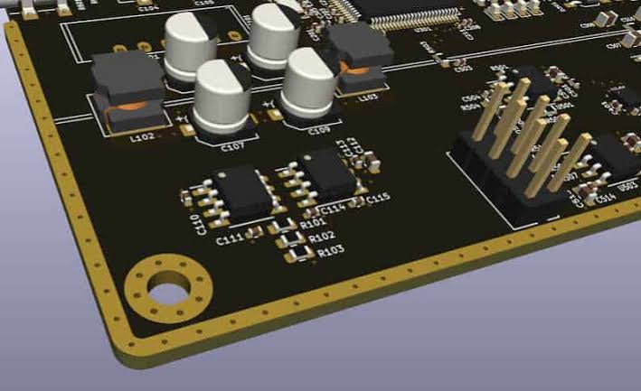
The quotation should identify which deliverables are included. Typical outputs may include source files, schematic PDFs, Gerber or ODB++ data, drill files, fabrication drawings, assembly drawings, BOM data and component coordinates.
The number of design reviews and permitted revisions should also be defined. Unlimited revisions can make a quotation appear flexible, but they leave both schedule and cost difficult to control.
Schematic Quality Changes the Layout Workload
A complete schematic should identify component values, part numbers, power networks, differential pairs and interface requirements. Unclear or incomplete circuit information forces the PCB designer to spend time resolving engineering questions before routing can begin.
PCB design cost may increase when the supplied schematic contains unverified footprints, inconsistent net names or missing power connections. These problems are not merely administrative. An incorrect footprint or pin assignment can make the first prototype unusable.
A schematic review should examine power architecture, decoupling, unused pins, connector assignments and programming access. Resolving these issues before placement is normally less expensive than modifying a routed board.
Placement and Routing Complexity Drive the Core Work
Component count matters because every device requires placement and electrical connections. Density matters more because components compete for limited routing, thermal and mechanical space.
A compact board may contain connectors with fixed positions, antennas with keep-out areas, processors requiring short memory routes and power devices requiring large copper regions. These constraints interact. Moving one component can affect several traces, return-current paths and thermal zones.
For this reason, pcb design cost rises when placement requires repeated optimization rather than simple component distribution. A dense board may also require smaller packages, microvias, via-in-pad structures or additional signal layers.
Routing effort is not determined only by the number of nets. Low-speed control signals can tolerate more routing variation than clocks, memory buses or high-speed differential interfaces. Critical connections must be prioritized before the remaining signals are routed.
The designer must also preserve space for assembly, inspection, testing and rework. A layout that connects every net but cannot be assembled economically is not production-ready.
Layer Count Is a Result Rather Than a Starting Number
Additional layers provide routing space and continuous reference planes, but each layer also affects fabrication cost. Selecting too few layers may force long routes, plane interruptions or impractical trace spacing. Selecting too many increases board cost without necessarily improving performance.
Stack-up development contributes to pcb design cost because the designer must coordinate signal layers, reference planes, power distribution, dielectric thickness and impedance requirements with a PCB manufacturer.
Layer transitions are also important. When a high-speed signal changes layers, its return current must move between reference structures. Poorly planned transitions can create larger current loops and increase electromagnetic emissions.
The final stack-up should represent both electrical requirements and available manufacturing processes. A theoretically ideal structure has limited value if it requires unusual materials or tolerances that make every production order expensive.
High Speed Interfaces Require More Engineering
High-speed design begins before routing. The designer must identify controlled-impedance nets, timing relationships, acceptable losses and the reference plane used by each signal group.
PCB design cost is higher when a board contains DDR memory, PCI Express, USB, Ethernet, MIPI or other fast interfaces. These signals may require differential-pair control, length relationships, via management and careful connector breakout.
The work is not simply matching visible trace lengths. Package delay, layer changes, reference discontinuities and coupling from neighbouring signals can all affect timing and signal quality.
Signal-integrity simulation may be included where interface speed and channel complexity justify it. Simulation adds engineering time, but it can expose routing problems before prototypes are manufactured.
IPC’s signal-integrity design syllabus connects advanced PCB work with manufacturing, packaging, routing and relevant design standards, illustrating why high-speed layout requires more than ordinary net routing.
Power and Thermal Requirements Affect Layout Time
High-current circuits require copper areas, vias and component placement that support both electrical delivery and heat removal. Voltage regulators, processors, power transistors and current-sense components often impose conflicting placement requirements.
A design may need short switching-current loops, separation from sensitive analogue signals and sufficient copper for heat spreading. Enclosure airflow and heatsink locations can restrict where components are placed.
The resulting pcb design cost reflects the analysis and iteration required to balance these constraints. If thermal simulation, power-integrity analysis or detailed current-density review is required, that work should appear explicitly in the quotation.
Ignoring these requirements may reduce the initial design fee but create a board that overheats or becomes unstable under full load.
Component Libraries Can Hide Significant Risk
Every schematic symbol and PCB footprint connects logical design data to a physical component. Library work includes pad dimensions, pin numbering, polarity, package outline, courtyard and assembly information.
PCB design cost increases when many components require new library creation. The work becomes more demanding for fine-pitch BGAs, bottom-terminated packages, unusual connectors and components with several package options.
Manufacturer-recommended land patterns are useful starting points, but they still require review against the intended assembly process. Thermal pads, solder-mask openings and stencil requirements may need project-specific adjustment.
A footprint should be verified before layout rather than after prototype assembly reveals a dimensional or pin-mapping error.
DFM Is Part of Design Rather Than a Final Check
Design for manufacturing examines whether the PCB can be fabricated and assembled with a stable process. It covers trace and spacing capability, drill dimensions, annular rings, copper balance, solder-mask features, component clearances and panelization constraints.
A DFM review may initially appear to increase pcb design cost, but it can prevent fabrication holds, assembly defects and repeated prototypes. The economic value lies in resolving problems while they still exist only in the design files.
IPC describes producibility levels as a way to communicate increasing difficulty in features, tolerances, assembly and testing. Higher sophistication generally requires more advanced tooling, materials or processing and can increase fabrication cost.
IPC-2231A also treats manufacturability, fabrication, assembly, testability, cost and reliability as connected parts of a formal Design for Excellence process.
Testability Changes Both Design and Production Cost
Test points require board area, but removing them can make programming and production diagnosis more expensive. Power rails, ground, reset, communication interfaces and critical analogue signals should remain accessible where practical.
If automated testing is planned, the PCB designer must understand probe access, fixture clearances and panel orientation. Boundary scan or functional test connectors may also require defined routing and placement.
These requirements add engineering work and influence pcb design cost, but they reduce dependence on manual troubleshooting during production. The goal is not to maximize the number of test points; it is to preserve access to signals that can isolate likely failures.
Documentation Determines Whether the Design Can Be Built
Routing completion is not the end of PCB design. Manufacturing data must communicate materials, dimensions, stack-up, impedance, tolerances, surface finish and special processes.
Assembly documentation should show component location, polarity and any special installation requirements. BOM, centroid data and drawings must correspond to the same revision.
Incomplete documentation may produce clarification delays or inconsistent interpretations between suppliers. Preparing a controlled production package contributes to pcb design cost because the designer must verify both the electrical layout and the information used to manufacture it.
Revisions Can Cost More Than the Initial Layout
A small schematic change introduced late in the project may affect placement, routing, planes and manufacturing outputs. The cost depends on the impact of the change rather than the number of edited schematic symbols.
Changing a connector can require mechanical review and rerouting. Replacing a BGA processor may alter hundreds of nets and the layer stack. Moving mounting holes can disturb copper and component clearances across several layers.
PCB design cost is easier to control when requirements, enclosure dimensions and major components are stable before detailed routing begins. Formal review points also prevent conflicting feedback from being introduced after different sections have already been approved.
How to Reduce Cost Without Weakening the Design
The most effective way to reduce pcb design cost is to reduce uncertainty. A complete schematic, approved BOM, accurate mechanical files and clear interface requirements allow the designer to begin with fewer unresolved decisions.
Using proven component libraries and standard manufacturing capabilities also reduces risk. Extremely small vias, narrow spacing and unusual stack-ups should be used only when the product requires them.
Early communication with the PCB fabricator and assembler can prevent layout rules from being based on unrealistic assumptions. At iPCB, a preliminary review can connect PCB design requirements with fabrication, assembly and testing capability before the layout is finalized.
Reducing review or verification merely to obtain a lower quotation can shift cost into prototypes and production. A cheaper design stage is not an economic advantage if the first assembly cannot be manufactured or tested reliably.
Evaluate the Work Behind the Quotation
A useful PCB design quotation should describe scope, deliverables, revision limits, technical assumptions and verification activities. Comparing only the final amount may hide significant differences in what each supplier is offering.
PCB design cost reflects the time required to resolve electrical, mechanical and manufacturing constraints before they become physical defects. Component density, high-speed interfaces, power delivery, library creation, DFM, testing and documentation all influence that effort.
The right pcb design cost is therefore not simply the lowest design fee. It is the cost of producing data that can move from prototype to repeatable manufacturing without avoidable redesign, production delays or reliability failures.