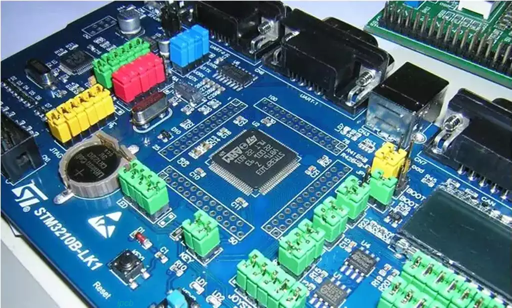
In the design and manufacture of printed circuit boards, the choice of layer count is never merely a numbers game—it directly affects the circuit’s electrical performance, immunity to interference and long-term reliability. 2 layer pcb and 4 layer boards, as the two most commonly used specifications, represent fundamentally different design philosophies and application boundaries. Understanding their fundamental differences not only helps engineers make more informed selection decisions at the project’s outset, but also enables them to avoid many circuit faults caused by improper stack-up design at the source.
Layer Stack Design
The core limitation of a 2 layer pcb lies in the simplicity of its layer stack structure—comprising only top and bottom copper foil layers. Consequently, all signal traces, power lines and ground lines are forced to share the limited space within these two layers. Whilst this layout may be feasible for simple circuits such as those found in toys or small sensors, in complex circuits such as those used in industrial control, consumer electronics and automotive electronics, it directly leads to routing congestion and cross-interference, becoming a key cause of circuit instability.
The routing challenges of 2 layer pcbs are evident in two key aspects: Firstly, trace crossing is unavoidable. To connect different components, traces often require repeated routing, which not only increases trace length and causes signal transmission delays, but also results in capacitive coupling between crossing traces, leading to signal crosstalk and causing signal distortion or false triggering; secondly, power and ground traces cannot be effectively separated; interference generated by power lines is directly conducted to ground lines, compromising ground stability and consequently affecting the signal integrity of the entire circuit. Particularly in high-frequency signal scenarios, the crowded routing on 2 layer pcb exacerbates interference issues.
The introduction of 4 layer board was specifically designed to resolve this routing dilemma. Their typical layer stack-up consists of ‘signal layer – power layer – ground layer – signal layer’ or ‘signal layer – ground layer – power layer – signal layer’. The two additional layers serve as independent power and ground planes, achieving a separate layout for ‘signal, power and ground’ – which is the most fundamental distinction from 2 layer pcbs.
This layered design transforms routing from ‘crowded and chaotic’ to ‘orderly and efficient’: signal traces can be concentrated on the top and bottom layers, whilst power and ground each have their own dedicated layers, eliminating the need to compete for space with signal traces and thereby reducing trace crossing and signal interference at the source.
More importantly, the independent ground layer in a 4 layer PCB forms a complete “ground plane”, effectively creating a stable “signal shield” for the entire circuit. The ground plane not only rapidly absorbs interference signals generated during signal transmission but also provides a stable return path for signal traces, reducing signal attenuation and enhancing the stability of signal transmission.
In contrast, 2 layer pcb, lacking a dedicated ground plane, can only employ ‘single-point grounding’ or ‘multi-point grounding’ methods. These result in poor grounding performance and an inability to effectively suppress interference—which is the fundamental reason why 2 layer pcbs are prone to signal distortion and circuit failure in high-frequency applications.
Immunity to Interference
In a 2 layer pcb, signal traces, power traces and ground traces are confined to the same layer, making it difficult to ensure adequate spacing between them. This results in capacitive and inductive coupling between adjacent traces, leading to signal crosstalk. For example, in the digital circuits of a 2 layer pcb , if high-frequency digital signal traces are too close to analogue signal traces, the high-frequency interference generated by the digital signals will affect the stability of the analogue signals, leading to signal distortion; meanwhile, ripple interference generated by power supply traces will also be conducted through the ground lines to the entire circuit, affecting the normal operation of components.
4 layer board fundamentally resolve internal crosstalk issues through dedicated power and ground planes. A dedicated power plane provides a stable and clean power supply to the entire circuit, reducing power supply ripple interference; the ground plane formed by the dedicated ground layer rapidly absorbs interference generated by signal traces whilst isolating different types of signals, thereby preventing crosstalk between them. Furthermore, signal traces on a 4 layer PCB can utilise a ‘microstrip’ or ‘stripline’ structure, which effectively controls impedance, reduces radiated interference during signal transmission, and further enhances signal integrity.
From an electromagnetic compatibility (EMC) perspective, 2 layer pcb lack a complete shielding structure, making it easy for external electromagnetic signals to penetrate the circuit and affect signal transmission; simultaneously, electromagnetic radiation generated within the circuit can leak outwards, affecting the normal operation of surrounding equipment and making it difficult to pass EMC testing.
In contrast, the independent ground plane of a 4-layer PCB acts as a complete shielding layer, effectively blocking the intrusion of external electromagnetic interference whilst suppressing the leakage of internal electromagnetic radiation. This significantly improves the circuit’s EMC performance, making it easier to pass relevant tests, and rendering it suitable for applications with high EMC requirements, such as automotive electronics, medical equipment and industrial control systems.
It should be noted that the anti-interference advantage of a 4 layer PCB is not simply a matter of ‘layers outnumbering’ the problem, but rather a structural advantage derived from the layered design. In practical design, the interference resistance of a 2 layer pcb can also be improved through optimised routing and the addition of ground copper foil.
However, the effectiveness of such optimisations is limited and cannot fundamentally address the structural shortcomings. When circuit complexity increases and signal frequencies exceed 100 MHz, the interference resistance advantages of a 4 layer PCB become even more pronounced, making it an essential choice for ensuring circuit stability.

Heat Dissipation and Mechanical Strength
Differences in heat dissipation performance stem from variations in copper foil area and laminate structure. In a 2 layer pcb,the copper foil is distributed only on the top and bottom layers, resulting in a limited heat dissipation area. When the circuit generates significant power—such as in high-power chips or LED driver circuits—heat cannot dissipate rapidly and accumulates on the board, causing component temperatures to rise and affecting circuit stability.
In contrast, 4 layer board feature dedicated power and ground planes with large-area copper cladding. The copper area is significantly greater than that of 2 layer pcbs. Given copper’s excellent thermal conductivity, heat generated by components is rapidly conducted throughout the board and then transferred via heat-dissipating vias and copper traces to the enclosure or heat sink, substantially improving heat dissipation efficiency.
In terms of mechanical strength, 4 layer board, due to the addition of two layers of substrate and copper foil, are thicker overall than 2 layer pcbs—conventional 2 layer pcbs are 1.6 mm thick, whilst 4-layer boards are typically 1.6 to 2.0 mm thick—and therefore possess greater mechanical strength and superior resistance to bending and deformation. Due to their thinner profile, 2 layer pcbs have lower mechanical strength and are prone to bending and deformation when subjected to external pressure during assembly, transport or use, leading to pad detachment or broken traces and resulting in circuit faults; whereas 4 layer boards have a more robust structure, effectively resisting external impacts and reducing circuit faults caused by mechanical damage, making them particularly suitable for scenarios involving frequent movement or vibration, such as portable devices and automotive electronics.
2 layer pcbs offer the advantages of low cost, simple design and short production cycles. They are suitable for applications with simple circuits, low power consumption and modest stability requirements, such as toy circuit boards, small sensors and basic control boards. For such applications, choosing a 2 layer pcb not only meets requirements but also keeps costs under control, making it the most cost-effective option.
However, when circuits meet the following criteria, the advantages of 4 layer board become apparent, making them an essential choice for ensuring circuit stability: firstly, high circuit complexity involving a large number of components and requiring dense routing, which 2 layer pcb cannot accommodate; secondly, high signal frequencies exceeding 100 MHz, demanding high signal integrity and anti-interference capabilities, such as in high-frequency communication and digital signal processing circuit boards; thirdly, circuits with high power consumption requiring excellent heat dissipation, such as high-power driver and power module boards; and fourthly, circuits with stringent requirements for electromagnetic compatibility and mechanical strength, such as automotive electronics, medical devices and industrial control boards.
The difference between 4-layer and 2 layer pcb is never as simple as ‘just having two extra layers’; rather, it represents a qualitative leap in circuit stability achieved through multiple aspects including stack-up design, interference resistance, heat dissipation and mechanical strength. These additional two layers accommodate more rational routing logic, stronger anti-interference capabilities and superior heat dissipation performance; they epitomise the PCB manufacturing industry’s evolution from ‘meeting basic requirements’ to ‘pursuing high quality and stability’.
The comparison between 2-layer and 4-layer boards essentially boils down to a balance between design redundancy and cost control. 2 layer pcb meet basic requirements with simplicity and practicality, whilst 4 layer boards leverage structural advantages to fulfil expectations of higher performance. When weighing up PCB options, there is no absolute superiority or inferiority; only the wisdom to determine the right fit for the application. When circuit complexity crosses a critical threshold, those two additional layers become the final line of defence for stability and the most solid guarantee of product quality.