Allflex PCB, also known as Flexible Printed Circuit Board (FPC), is a type of circuit board that can be completely bent. Folded or curled circuit board. It consists of one or more layers of polyimide film as a substrate, covered with a copper foil layer and a cover film, and the circuit pattern is formed by etching or printing.
AllflexPCB Design Considerations Required
AllflexPCB Layout Guidelines
1.Components should be placed in the rigid board area, while the flexible board will only take on the connecting function, so as to extend its bending life and thus improve the reliability of the product. If the components are placed directly in the flexible board area, it may lead to cracked pads, damage or character removal.
2.While placing components in the rigid board area, make sure that they are at least 1mm away from the edge of the rigid-flex area.
3.When the flexible area needs to be extended to the rigid area, the minimum distance between the two should be maintained at 1mm or more.
Allflex PCB wiring requirements
1.Allflex pcb area line alignment direction perpendicular to the bending line,in order to prevent bending test graphics along a certain direction of cracking, bending line alignment can be used to connect the arc.
2.Flexible board area graphics from the edge of the PCB board at least 10mil,can not be punched, the distance between the hole and the combination of hard and soft at least 2mm.
3.If the allflex pcb area has an internal electric layer, without affecting the power supply connection. Current value. Impedance value of the case, can be placed in the flexible board area to isolate, improve the softness of the soft area.
4.Add soft zone identification in the soft zone part of the mechanical auxiliary layer, which can be easily distinguished during production.
5.In case of impedance design and impedance lines need to be placed in the soft zone, it is necessary that the soft zone wiring layer must have a corresponding reference layer on each monolithic chip when the impedance structure diagram is developed.
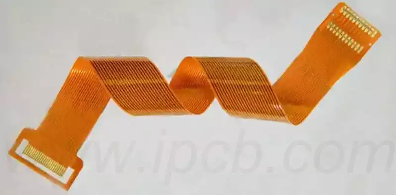
The design of FPC stacking structure is closely related to its performance and application scenarios. So, how to choose the right stacking structure for FPC?
Single-layer board
Single-layer board is the most basic structure of FPC, which is made of single-sided copper-clad board with conductive lines on one side only. After processing, a protective film or coating will be added to the surface to strengthen the insulation and protection of the line. This structure is suitable for simple circuit connections with low wiring density.
Standard double-sided boards
Compared to single-layer boards, standard double-sided boards have conductive wiring on both sides and are covered with a protective film, forming a circuit board with two layers of conductors. This structure significantly increases wiring density and is ideal for complex circuit systems that require more interconnections.
Partially Laminated Single Layer Boards (Substrate Window Laminates)
Partial Lamination Monolayer is a specially designed FPC that uses two layers of single-sided copper-clad laminate, which are partially laminated by bonding adhesive with windows at specific locations. This design allows the FPC to have higher flex performance in the delamination area while maintaining the double-layer conductor structure in other areas, making it ideal for application scenarios that require localised high flexibility.
Multilayer boards
Multilayer boards are an advanced form of FPC, in which a multilayer conductor structure is formed by repeatedly laminating a single-side copper-clad laminate and bonding adhesive. This design not only greatly improves the wiring density and signal transmission efficiency, but also optimises the flexing performance by designing the local layer structure to meet the needs of high-performance and high-complexity electronic devices.
Rigid-Flex PCB (Rigid-Flex PCB)
Rigid-flex bonded boards are a perfect combination of FPC and rigid circuit boards (PCBs). Rigid and flexible substrates are selectively bonded together through a lamination process, and conductive connections are achieved through metallised holes. This structure retains the flexibility of an FPC with the high strength and stability of a PCB, and is widely used in electronic products that require high integration, high reliability and complex bending requirements, such as smartphones, tablets and wearable devices.
Allflex pcb plays a key role in many areas, the following are its main application areas:
Consumer Electronics: Allflex pcb is an important component of products such as smartphones, tablets, wearables (e.g., smartwatches and health monitors), digital cameras, and headphones. They help these devices achieve thinner, more compact designs and provide sophisticated circuit connection solutions in limited spaces.
Communications: FPCs are used for antenna connections, internal signal transmission, and high-speed data transmission in applications such as wireless communications equipment, 5G infrastructure, and mobile network equipment, especially in space-constrained environments.
Medical Devices: FPCs are used in a wide range of medical devices, such as endoscopes, cardiac monitors, portable medical testing instruments, and medical devices that need to be implanted in the human body or used close to the skin, thanks to their bendability and miniaturisation.
Automotive electronics: In modern automotive manufacturing, allflex pcb is used to connect complex electronic control systems, including navigation systems, lighting control, sensor networks and driver assistance systems, etc., especially in those parts that need to adapt to vehicle motion and vibration, its performance is particularly good.
Aerospace: In spacecraft and aircraft, FPCs are able to withstand extreme environmental conditions such as temperature variations, vibrations and differences in air pressure, making them widely used in critical areas such as flight control,communication systems and sensor networks.
With its superior flexibility and wide range of applications, allflex PCB is becoming an integral part of modern electronic equipment. From sophisticated consumer electronics to complex aerospace systems, allflex pcb has demonstrated its unique value and potential.
